8.3 TIMER0 Related Register
There are two registers related to TIMER0, 8-bit timer/counter (TMR0), and 8-bit programmable control
register (OPTION_REG).
TMR0 is an 8-bit readable and writable timer/counter, OPTION_REG is an 8-bit write-only register, the
user can change the value of OPTION_REG to change the working mode of TIMER0, etc. Please refer to the
application of 0 prescaler register (OPTION_REG).
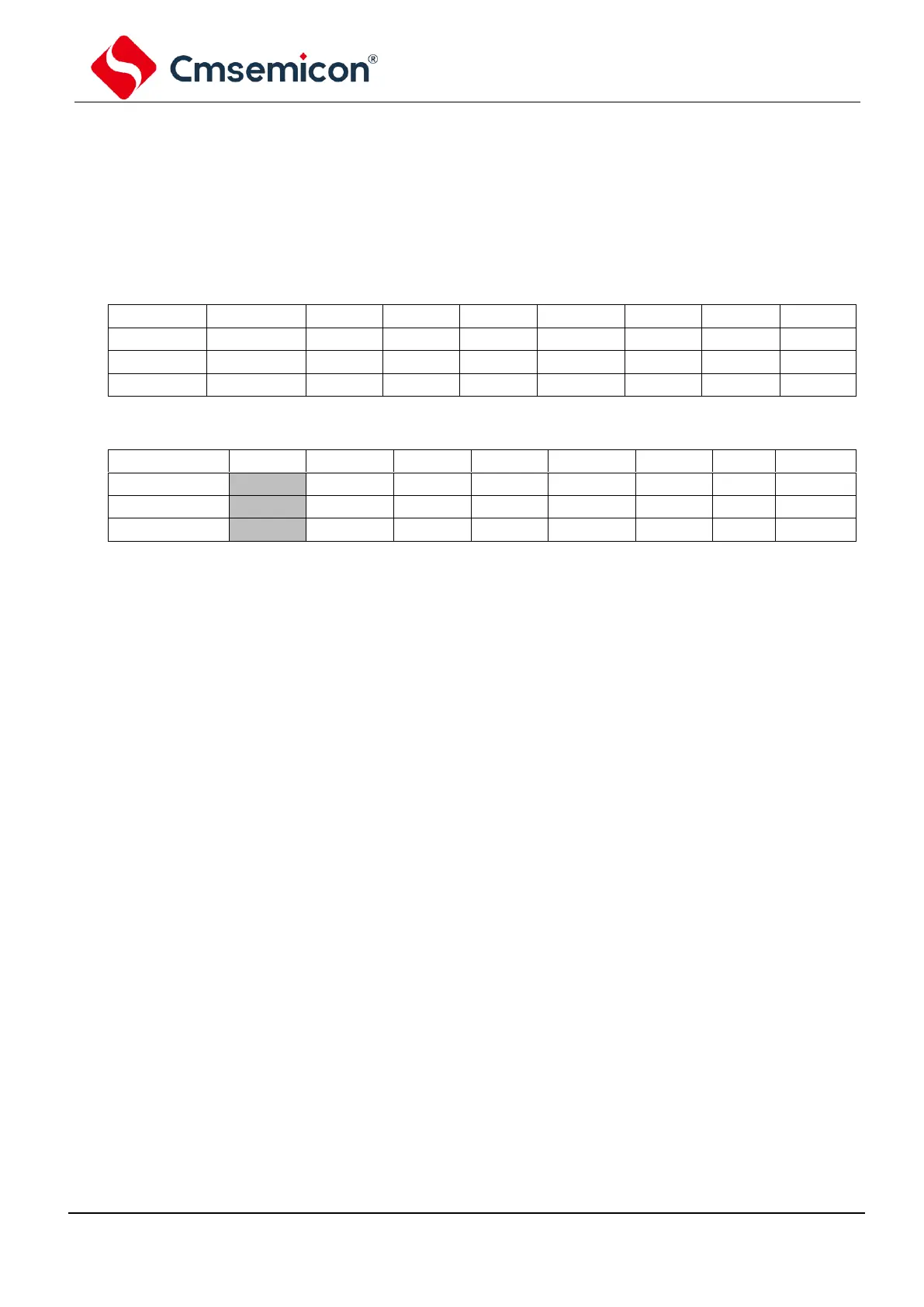
8-bit timer/counter TMR0 (01H)
OPTION_REG register (81H)
Interrupt edge selection bit.
The rising edge of the INT pin triggers interrupt.
The falling edge of the INT pin triggers interrupt.
TMR0 clock source selection bit.
Transition edge of T0CKI pin.
Internal instruction period clock (
F
CPU).
TIMER0 clock source edge selection bit.
Increment when the T0CKI pin signal transitions from high to low.
Increment when the T0CKI pin signal transitions from low to high.
pre-scaler allocation bit.
pre-scaler allocated to WDT.
pre-scaler allocated toTIMER0 mod.
Pre-allocated parameter configuration bits.
TMR0
Frequency
division ratio
WDT Frequency
division ratio
(WDT_DIV=DISABLE)
WDT Frequency
division ratio
(WDT_DIV=ENABLE)