8525B/8528 Technical Service Manual Technical Description 4-19
Publication No: 15-02036 Issue 6
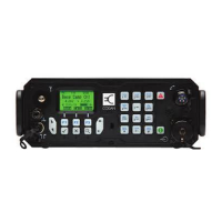
4.7.2 Switch Matrix
The switches on the panel overlay (substrate) form a 4 x 4 matrix. The row
and column connections are taken to the Display PCB. (A table listing the
switch functions and corresponding connections is given in Section 6.2.3.)
The row connections are polled by the microprocessor, via IC2 by taking
them to 0V one at a time. A switch operation is detected by the
corresponding column connection to IC4 going to 0V. Data indicating the
switch closure is encoded and returned, via the I
2
C bus, to the
microprocessor.
4.7.3 Digiswitches (8525B)
Transceivers and control heads fitted with selective call mesh (SDEM) have
thumbwheel digiswitches on their front panels. The BCD outputs of these
are applied to the Display PCB. Individual switches are polled so that switch
settings are detected and returned to the microprocessor in a similar way to
the matrix switches.
4.7.4 Microphone Amplifier and Interface (04-02096)
To compensate for the long lines connecting the Control Head to the
transceiver, a Microphone Amplifier and Interface (08-03039), interfaces the
Display PCB with the lines to the transceiver. On entering the board each
line is filtered to prevent interference picked up on the lines from affecting
the operation of the head.
The board contains buffers for the Data, Clock and Enable lines of the data
bus. A 3-terminal regulator, IC1, on the A rail provides the 5V supply for
use by these buffers and the Display PCB.
An amplifier formed by IC3 and its associated components amplifies the
microphone input to a suitable level for application to the lines. V2 on the
input to the amplifier operates as a clamp in the same way as V7 on the
Audio and IF 1650kHz PCB. This circuit is powered by a separate 10V
supply derived from the A rail by zener diode V1.