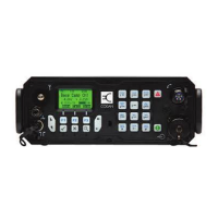
4-10 Technical Description 8525B/8528 Technical Service Manual
Issue 6 Publication No: 15-02036
When the phase/frequency difference is considerable, e.g. immediately after
a change of channel, the output from PDB (IC5 pin 2) consists of pulses
with their mark:space ratio proportional to the difference. These are
integrated by R82 and C123 to provide an input to IC2b. The signal is
further filtered by R85 and C127, while the output from IC2b is filtered by
R90, R91, C131, C132, C133 and C134. At the same time PBA pin 1 gives
an analogue output proportional to the phase/frequency difference. This is
also applied to the input of IC2b, via R80. The resulting output drives VCO1
in the direction required to obtain the correct frequency, thus providing a
coarse control of the frequency.
When the phase/frequency difference becomes small the PDB output goes
high impedance and the analogue output from PDA becomes the only input
to IC2b. This provides the fine control of the VCO1 output.
IC7 generates the DC voltage required to control the varicaps in VCO2. A
similar arrangement of prescaler and internal dividers divides the VCO2
output in the same way as VCO1 was divided in IC5. The result is compared
with a reference frequency within IC7. The 6.6MHz crystal oscillator output
from IC5 is applied in IC7 to a divider which can be programmed to provide
reference frequencies between 1.1 and 2kHz. This allows VCO2 frequency
to be changed in 10Hz steps.
Coarse control of VCO2 is provided by the Freq output (pin 6) from IC7.
This consists of low pulses if the VCO frequency is too high, and high
pulses if it is too low. These are integrated in C147 to provide the correcting
voltage to VCO2. Fine control is provided by the Phase output (pin 17).
4.4.3 Lock Signals
Both phase/frequency detectors give an output which is low while the VCO
and reference frequencies are locked, and high when they are unlocked. The
LD output from IC5 pin 3 is applied to the base of V28 and the Charge
output from IC7 pin 4 is applied to V29. Thus the corresponding transistor is
switched on to light the LED indicator (H1 or H2) in its collector circuit if
either loop loses lock. The collector circuits are ORed by D45 and D46 so
that if either collector is low, i.e. one loop has lost lock, an Unlock output is
passed to the Microprocessor Controller PCB.
4.4.4 Loading Frequency Data to Synthesizers
Data containing the required division factors for both synthesizers is applied
from the Microprocessor Controller PCB over the Data line. The serial data
is clocked into IC7 under the control of the signal on the clock line. The first
twenty-eight bits are clocked through IC7 and into IC5, via SR Out (pin 14)
of IC7. When the twenty-eight bits have been clocked they are loaded in IC5
by the Enable 1 pulse from the Microprocessor Controller PCB. Similarly
the next thirty-two bits are loaded into IC7 by the Enable 2 pulse.