8525B/8528 Technical Service Manual Maintenance 6-7
Publication No: 15-02036 Issue 6
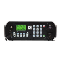
Front Panel Switch Tests (8525B)
Connector Pin 8525B
1 - 5 Scan
1 - 6 Audio Mute
1 - 7 S’call Mute
1 - 8 Power On/Off
2 - 5 Tune
2 - 6 Mute off
2 - 7 USB/LSB
2 - 8 Emgcy Call
3 - 5 Clarifier
3 - 6 Channel
3 - 7 Channel
3 - 8 Call
4 - 5 Clarifier
4 - 6 Volume
4 - 7 Volume
4 - 8 -
6.2.4 Logic Levels
If the switches are found to be satisfactory, the lack of response may be
caused by faults in the main microprocessor or the associated data buses. If
this type of fault is encountered, the I
2
C bus lines should be monitored with
an oscilloscope. This can be done at J1 pins 1 to 4 and P3 pins 1 to 3 on the
Microprocessor Controller PCB. Operation of any of the front panel controls
should cause the exchange of data via the bus lines. This should be seen on
the oscilloscope as rapidly changing levels between +5 and 0V. No data on a
line, or failure of the levels to change cleanly should be investigated further.
Failure may be due to an IC or its load. Refer to 6.2.1. Ensure that the
terminations of all interconnecting ribbon cables are correctly mated and
aligned.
6.2.5 No Reception
If no signal is received, after confirming the supply voltages described in
6.2.2, the signal path should be traced back from the output stages by
applying the appropriate signals at convenient points. Voltages to be
expected at various points are shown in the circuit diagrams.
 Loading...