TABLE OF CONTENTS
1. 1101/1201 GENERAL SPECIFICATIONS........................................................................................ 3
2. TROUBLESHOOTING....................................................................................................................... 4
2.1 P
ROBLEMS DURING INITIAL
D
OCKSIDE
S
ETUP
:................................................................................ 4
2.2 C
IRCUIT
B
OARD
R
EPAIRS
:............................................................................................................... 4
3. CIRCUIT DESCRIPTION.................................................................................................................. 5
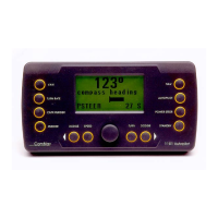
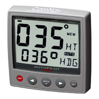
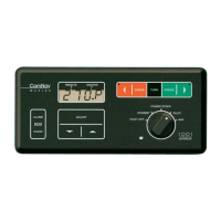
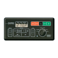
3.1 HEAD............................................................................................................................................. 5
3.1.1 General Description:.................................................................................................................. 5
3.1.2 Disassembly/Re-Assembly .......................................................................................................... 5
3.1.3 Button Replacement:................................................................................................................... 5
3.2 1101 SPU
PN
82888 R
EV
. 2 (2
PCB VERSION
)................................................................................ 6
3.2.1 General Description:.................................................................................................................. 6
3.2.2 Disassembly/Re-assembly (2 pcb version).................................................................................. 7
3.2.3 Signals to and from the Distribution Unit ..................................................................................7
3.2.4 Signals to and from the Control Head........................................................................................ 7
3.2.5 Signals to and from the Compass ............................................................................................... 8
3.2.6 Signals to and from the Remotes ................................................................................................ 8
3.3 1101/1201 SPU............................................................................................................................... 9
F
OR
1101:
PN
82888 R
EVISION
3 (1
PCB VERSION
) ..................................................................................... 9
F
OR
1201:
PN
83747 R
EVISION
1 (1
PCB VERSION
) ..................................................................................... 9
3.3.1 General Description:.................................................................................................................. 9
3.3.2 Disassembly/Re-assembly (1 pcb version).................................................................................. 9
3.3.3 Signals to and from the Distribution Unit ..................................................................................9
3.3.4 Signals to and from the Control Head...................................................................................... 10
3.3.5 Signals to and from the Compass ............................................................................................. 10
3.3.6 Signals to and from the Remotes .............................................................................................. 10
3.3.7 Signals from the SERIAL DATA Output................................................................................... 11
4. CONNECTIONS ................................................................................................................................ 12
4.1 R
EMOVING
C
ONNECTORS FROM THE
SPU..................................................................................... 12
4.2 R
EMOVING THE BACK SHELL TO VIEW THE WIRES
......................................................................... 13
4.3 H
EAD TO
SPU ............................................................................................................................... 14
4.4 D
ISTRIBUTION
B
OX TO
SPU.......................................................................................................... 15
4.5 C
OMPASS AND
S
ERIAL
D
ATA CONNECTIONS TO
SPU.................................................................... 16
5. DEALERS TEST BENCH................................................................................................................. 17
6. FINAL TEST PROCEDURE ............................................................................................................ 18
7. APPENDIX A...................................................................................................................................... 21
7.1 P
ROBLEM
S
OLVING
G
UIDE
F
ORM
.................................................................................................. 21
8. APPENDIX B...................................................................................................................................... 22
8.1 SPU D
RAWINGS
/S
CHEMATICS FOR
82888
REV
2, (2 PCB V
ERSION
)............................................ 22
8.1.1 Processor Board (B Board)...................................................................................................... 22
8.1.2 Backplane Board (C Board)..................................................................................................... 22
9. APPENDIX C...................................................................................................................................... 23
9.1 SPU D
RAWINGS AND
S
CHEMATICS FOR
82888
REV
. 3
AND
83747 (1
PCB VERSION
) ................... 23
9.1.1 Bill of Materials........................................................................................................................ 23
9.1.2 Board Layout............................................................................................................................ 23
9.1.3 Schematic.................................................................................................................................. 23