Service Manual
8
The over-voltage protection feature is implemented by using an extermal capacitor
devider(C1/C15/C16/C17) to sense the output voltage.The divide-down voltage signal is sent to the IC
Pin1(VSEN) ,thus regulating the output voltage.
If a CCFL is removed, fails or damaged during normal operation, CCFL current is no longer sensed and
the voltage on ISEN pin drops. The voltage at the SSTCMP(pin2)rises rapidly because there is no current
feedback at ISEN(pin14).When the voltage at SSTCMP reaches a threshold of approximately 2V and ISEN
is less than 0.7V,a current source charges the capacitor(C3) connected to TIMER(pin12).Once the voltage
level at the TIMER pin reaches a threshold of approximately 3V,the drive outputs shut down and latch.To
resume operation,toggle the ENA signal or restart VDDA.
Over-voltage and over-current protection are monitored by the voltage on VSEN(pin1).During normal
operation,if a CCFL is damaged or removed,the voltage at VSEN exceeds the user-defined, preset voltage
set by OVPT(pin15),the driver output duty cycle is regulated and the shutdown delay timer is
activated.OVPT sets the overall protection threshold voltage that is lower than3V(VSEN threshold. Once
the voltage at TIMER pin reaches 3V,the IC will shut down and latch. OVPT voltage setting is determined
by a resistor divider(R16/R8)connected to the OVPT.
2.2.Power PWM circuit
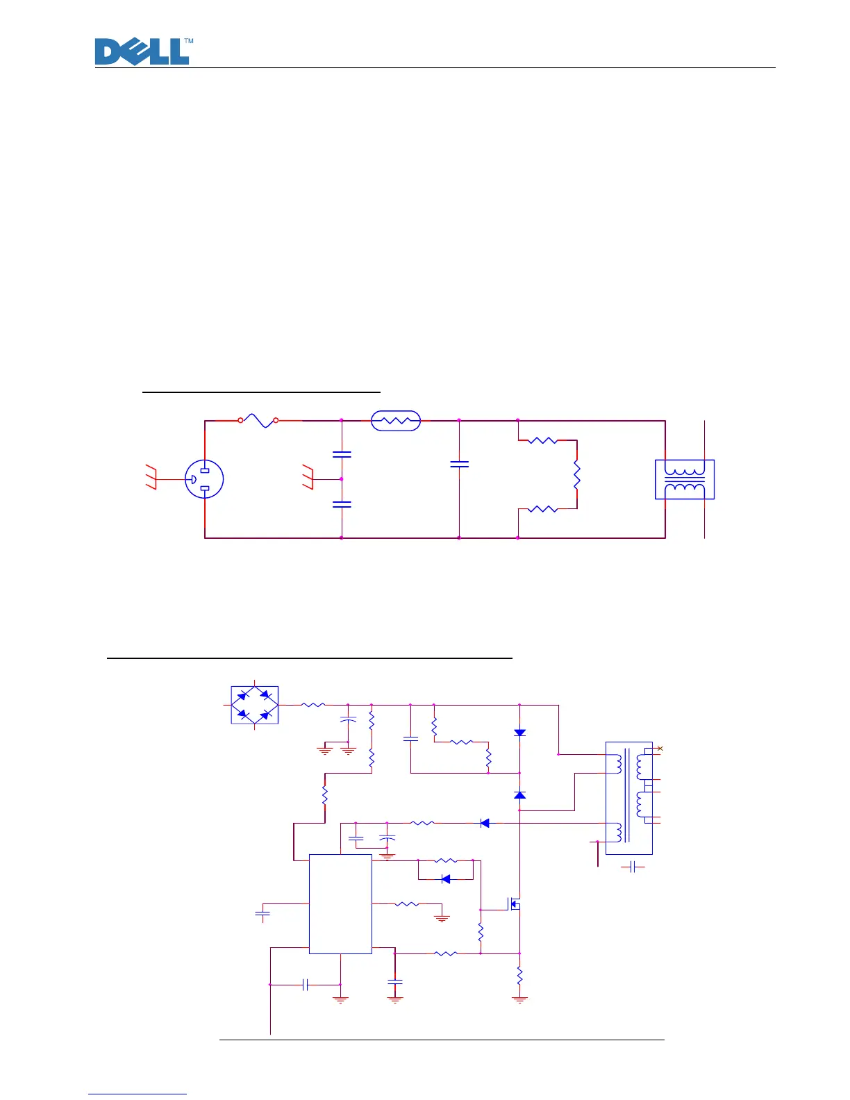
2.2.1 AC Input and EMI Filter:(fig.2.2.1)
R850
499K
F850
3.15A 250V
C850
222 Y2
L850
CHK-007
41
32
C851
222 Y2
R851
499K
C852
0.47uF X2
CN850
10A/250V
13
2
R852
499K
RT850
5R4A
fig.2.2.1
CN850 is a connector for connecting AC Power. F850 is a fuse to protect all the circuit AC. Input
voltage is from 90V to 264V. R850,R851and R852 are joined between two inputting main circuit to
prevent man from shock. L850 is used to clear up low frequency wave. C850 and C851 are used to
discharge the waves that L850 produced. High frequency waves are damped by C852.
2.2.2 High Voltage to Low Voltage Control Circuit:(fig.2.2.2)
R842
499K
C875
472P
R844 47R
Q850
AP2761
2
13
Signal_GND
R843
499K
U850
LD7552B
1
45
2
83
7
6
GND
RTNC
COMP
OUTVCC
VCC
CS
D852
SF10-04
C854
100uF/450V
R853
27K
.
.
.
T850
SPW-115
5
8
6
7
3
1 1