35
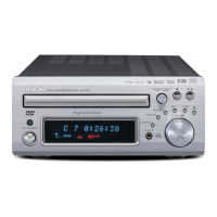
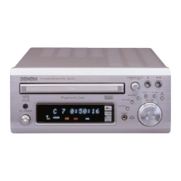
ADV-700
20
10
7
6
5
4
3
2
1
8
9
30
11
18 16 15 14 13 12 32 31
19
27
28
24
25
21
22
23
26
17
FG2
FG
H1H
H1L
H2H
H2L
H3H
H3L
VHB
EC
ECR
BMS
START
GND
CS1
CS2
A32
A31
A22
A21
A12
A11
VM2
VM1
VLP
VPUMP
BC1
BC2
BC3
BC4
VDD
Hall
Bias
X5
CSOUT
SRESET
PWMOUT
VCL
VT
OSC
Hall Amp
Matrix
Pre-Driver
Start/Stop
Logic Circuit
Booster
Thermal
Protect
Divider
3ø Bridge
Direction
SW
28
27
26
25
24
23
22
21
20
19
18
17
16
15
1
2
3
4
5
6
7
8
9
10
11
12
13
14
MUTE
BIAS
VINTK
CTKerr1
CTKerr2
VINLD
PreGND
PVcc2
VNFTK
PGND
VOLD-
VOLD+
VOTK-
VOTK+
VINFC
CFCErr1
CFCErr2
VINSL+
VINSL-
VOSL
VNFFC
PreVcc
PVcc1
PGND
VOSL-
VOSL+
VOFC-
VOFC+
BA5952AFP (DVD: IC504)
Terminal Function
Pin No. Name Function
1
2
3
4
5
6
7
8
9
10
11
12
13
14
CFCerr1
CFCerr2
VINSL+
VINSL-
VOSL
VNFFC
PreVcc
PVcc1
PGND
VOSL-
VOSL+
VOFC-
VOFC+
Focus driver input
Cap.connecting pin for error amp filter
Cap.connecting pin for error amp filter
Op.amp input (+) for sled driver
Op.amp input (-) for sled driver
Op.amp output for sled driver
Focus driver feedback pin
Pre Vcc
Power Vcc of sled driver
Power GND of sled driver
Sled driver output(-)
Sled driver output(+)
Focus driver output(-)
Focus driver output(+)
15
16
17
18
19
20
21
22
23
24
25
26
27
28
VOTK+
VOTK-
VOLD+
PGND
VNFTK
PVcc1
PreGND
VINLD
CTKerr2
CTKerr1
VINTK
BIAS
Tracking driver output(+)
Tracking driver output(-)
Loading driver output(+)
Loading driver output(-)
Power GND
Tracking driver feedback pin
Power GND
Pre GND
Loading driver input
Cap.connecting pin for error amp filter
Cap.connecting pin for error amp filter
Tracking driver input
Bias input
Mute control pin
Pin No. Name Function
VINFC
VOLD-
MUTE
SN74AHCT273PW (DVD: IC105) S-24C01A (DVD: IC108)
Truth Table
Input
Function
Output
D
CK QCLR
L
H
H
H
X
L
H
X
L
L
H
Qn
X
Clear
¾
¾
No change
X: Don't Care
Terminal Function
Name
Function
A0
A1
A2
GND
SDA
TEST/WP
Address input
GND
Serial data input/output
Test, connect to GND
Pin No.
1
2
3
4
5
6
7
8
SCL
Vcc
Address input
Address input
Serial clock input
Power supply
1
2
3
4
8
7
6
5
A0
A1
NC
GND
Vcc
TEST/WP
SCL
SDA
1
2
3
4
5
6
7
8
10
9
20
19
18
17
16
15
14
13
12
11
CLR
Q1
D1
D2
Q2
Q3
D3
D4
Q4
GND
Vcc
Q8
D8
D7
Q7
Q6
D6
D5
Q5
CK
1
16
32 17
AN8471SA (DVD: IC503)
Pin
Name
Function
Pin
No.
1 VHB Hall bias pin
2 H3L Hall element 3 input (-)
3 H3H Hall element 3 input (+)
4 H2L Hall element 2 input (-)
5 H2H Hall element 2 input (+)
6 H1L Hall element 1 input (-)
7 H1H Hall element 1 input (+)
8 EC Torque command input pin
9 ECR Torque command ref. input pin
10 FG1 FG signal lout put pin (0.C)
11 START Start/Stop switching pin
12 VPUMP Booster pin
13 BC1 Booster cap. connecting pin 1
14 BC2 Torque command input pin 2
15 BC3 Torque command input pin 3
16 BC4 Torque command input pin 4
17 GND GND pin
18 VDD Power pin
19 VM2 Motor power pin 2
20 FG2 3x FG signal output pin (0.C)
21 A31 Drive output 3
22 A32 Drive output 3
23 CS2 Current detect pin 2
24 A21 Drive output 2
25 A22 Drive output 2
26 CS1 Current detect pin 1
27 A11 Drive output 1
28 A12 Drive output 1
29 NC N.C.
30 BMS Brake mode switching pin
31 VM1 Motor power pin 1
32 VLP Pre-driver lower power
Terminal Function
w
w
w
.
x
i
a
o
y
u
1
6
3
.
c
o
m
Q
Q
3
7
6
3
1
5
1
5
0
9
9
2
8
9
4
2
9
8
T
E
L
1
3
9
4
2
2
9
6
5
1
3
9
9
2
8
9
4
2
9
8
0
5
1
5
1
3
6
7
3
Q
Q
TEL 13942296513 QQ 376315150 892498299
TEL 13942296513 QQ 376315150 892498299
http://www.xiaoyu163.com
http://www.xiaoyu163.com
 Loading...