EasyManua.ls Logo

Denon AVR-1804

Denon AVR-1804
89 pages
To Next Page IconTo Next Page
Loading...
SERVICE MANUAL
MODEL
AVR-1804/884
AVC-1880
AV SURROUND RECEIVER / AMPLIFIER
16-11, YUSHIMA 3-CHOME, BUNKYOU-KU, TOKYO 113-0034 JAPAN
X0173V.01 DE/CDM 0307
For U.S.A., Canada, Europe, U.K.,
Asia, China,Taiwan R.O.C., Korea
& Japan model
サービスをおこなう前に、このサービスマニュアルを
必ずお読みください。本機は、火災、感電、けがなど
に対する安全性を確保するために、さまざまな配慮を
おこなっており、また法的には「電気用品安全法」に
もとづき、所定の許可を得て製造されております。
従ってサービスをおこなう際は、これらの安全性が維
持されるよう、このサービスマニュアルに記載されて
いる注意事項を必ずお守りください。
本機の仕様は性能改良のため、予告なく変更する
ことがあります。
Please use this service manual with referring to the
operating instructions without fail.
Some illustrations using in this service manual are
slightly different from the actual set.
修理の際は、必ず取扱説明書を参照の上、作業を
行ってください。
本文中に使用しているイラストは、説明の都合上
現物と多少異なる場合があります。
補修用性能部品の保有期間は、製造打切後8年です。
注 意

Other manuals for Denon AVR-1804

Question and Answer IconNeed help?

Do you have a question about the Denon AVR-1804 and is the answer not in the manual?

Denon AVR-1804 Specifications

General IconGeneral
BrandDenon
ModelAVR-1804
CategoryReceiver
LanguageEnglish

Summary

SERVICE MANUAL INTRODUCTION

MODEL IDENTIFICATION

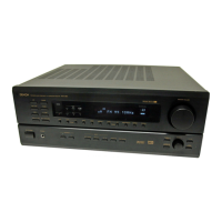
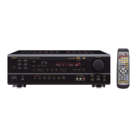
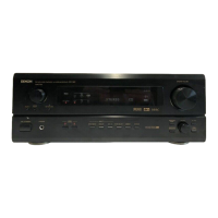
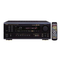
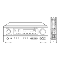
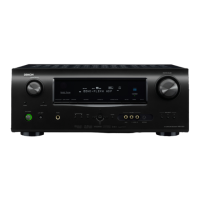
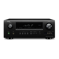
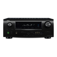
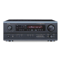
AVR-1804/884 AVC-1880 AV Surround Receiver / Amplifier.

GENERAL CAUTIONS

General warnings for service personnel regarding manual use and specifications.

SAFETY PRECAUTIONS

LEAKAGE CURRENT CHECK AND SAFETY GUIDELINES

Critical electrical safety checks and general precautions.

SAFETY CRITICAL PARTS IDENTIFICATION

Notes on parts essential for maintaining safety.

SIGNAL LEVEL DIAGRAMS

AUDIO CHANNEL SIGNAL FLOWS

Visualizes signal paths for front, center, and surround audio.

SUBWOOFER CHANNEL SIGNAL FLOW

Visualizes signal path for the subwoofer audio channel.

BLOCK DIAGRAM

ADJUSTMENT PROCEDURES

TUNER SECTION ALIGNMENT

Steps for calibrating FM and AM tuner performance.

AUDIO SECTION ADJUSTMENT

IDLING CURRENT SETTING

Procedure to set audio output idle current for optimal performance.

SEMICONDUCTOR COMPONENTS

MAJOR IC TERMINAL FUNCTIONS

Pinout and function descriptions for key integrated circuits.

FRONT PANEL DISPLAY

FL DISPLAY PIN AND GRID CONFIGURATIONS

Mapping of display pins to functions and grid assignments.

PRINTED WIRING BOARD LAYOUTS

MAIN P.W.B. UNIT LAYOUT

Component placement diagram for the main board.

CPU P.W.B. UNIT LAYOUT

Component placement diagram for the CPU board.

CNT P.W.B. UNIT LAYOUT

Component placement diagram for the control board.

INPUT-PRE AMP P.W.B. UNIT LAYOUT

Component placement diagram for the input pre-amplifier board.

DSP P.W.B. UNIT LAYOUT

Component placement diagram for the DSP board.

C-VIDEO P.W.B. UNIT LAYOUT

Component placement diagram for the C-Video board.

PARTS LIST GUIDANCE

COMPONENT SPECIFICATION DEFINITIONS

Explanations of resistor and capacitor coding and specifications.

P.W.B. UNIT PARTS LISTS

MAIN P.W.B. UNIT COMPONENTS

Detailed list of parts for the main circuit board.

CNT P.W.B. UNIT COMPONENTS

Detailed list of parts for the control circuit board.

INPUT P.W.B. UNIT COMPONENTS

Detailed list of parts for the input circuit board.

OTHER PARTS GROUP LIST

List of miscellaneous parts not specific to a single board.

C-VIDEO P.W.B. UNIT COMPONENTS

Detailed list of parts for the C-Video circuit board.

EXPLODED VIEWS

MODEL-SPECIFIC EXPLODED DIAGRAMS

Visual assembly guides for different regional model variations.

PARTS LIST OF EXPLODED VIEW

P.W.B. ASSEMBLY CROSS-REFERENCE

List of circuit board assemblies and their regional applicability.

SCREWS LIST AND SPECIFICATIONS

Detailed listing of screws used in the unit.

PACKING VIEW

PACKING CONTENTS DIAGRAM AND LIST

Visual and itemized list of items included in the product packaging.

PARTS LIST OF PACKING & ACCESSORIES

WIRING DIAGRAM

SCHEMATIC DIAGRAM INTERPRETATION

NOTES AND WARNINGS FOR SCHEMATICS

Important information, warnings, and notices for understanding circuit diagrams.

SCHEMATIC DIAGRAMS

INPUT BD SCHEMATIC

Detailed circuit diagram for the input board.

DSP UNIT SCHEMATIC

Detailed circuit diagram for the Digital Signal Processor unit.

CONNECTION CNT PRE AMP UNIT SCHEMATICS

Circuit diagrams for connection, control, and pre-amplifier units.

MAIN BD SCHEMATIC

Detailed circuit diagram for the main board.

CPU BD CPU-CNT UNIT SCHEMATICS

Circuit diagrams for CPU and CPU-CNT boards.

VIDEOBD C-VIDEO UNIT SCHEMATICS

Circuit diagrams for Video and C-Video boards.

COMPONENT-VIDEO TUNER UNIT SCHEMATICS

Circuit diagrams for component video and tuner units.

1 CH-AMP D-VIDEO UNIT SCHEMATICS

Circuit diagrams for 1-channel amplifier and D-Video units.

FRONT SWITCH HEAD PHONE FRONT-S-VIDEO UNIT SCHEMATICS

Circuit diagrams for front panel related units.

TUNER BD SCHEMATIC

Circuit diagram for the tuner board.

Related product manuals