21
21
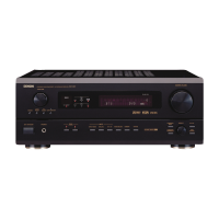
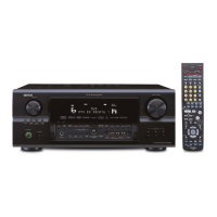
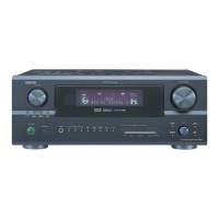
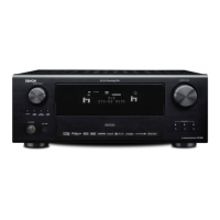
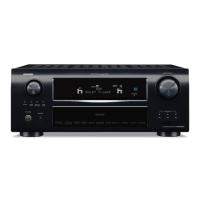
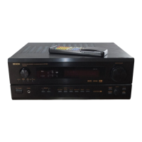
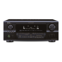
AVR-2803/983/AVC-2870
31
32
33
34
35
36
37
38
39
40
41
42
43
44
45
46
47
48
49
50
51
52
53
54
55
56
57
58
59
60
61
62
63
64
Pin
No.
PinName FunctionI/O
Symbol
Type
Det
Op
(Int.)
Op
(Ext.)
Res
P03/AD3 I/O4 I/O C Z DSPcomm.pin(ADSP21161N:D19)
P04/AD4 I/O5 I/O C Z DSPcomm.pin(ADSP21161N:D20)
P05/AD05 I/O6 I/O C Z DSPcomm.pin(ADSP21161N:D21)
P06/AD06 I/O7 I/O C Z DSPcomm.pin(ADSP21161N:D22)
P07/AD07 I/O8 I/O C Z DSPcomm.pin(ADSP21161N:D23)
P10/AD8/A8 ROMRST1 O C Ed Z MemoryresetforDSP(Reset:L)
P11/AD9/A9 DSP1RS O C Ed Z DSPresetoutputpin(Reset:L)
P12/AD10/A10 DSPI/0POWER O C Eu Z Poweron:L(10mslateronafterdigitalpoweron)
P13/AD11/A11 DSPOSCON O C Z ON:H(20mslateronafterdigitalpoweron)
P14/AD12/A12 IRQ1B1(DSPREQ1) O C Z
DSP(ADSP21161L‑A:IRQ1)hostI/Finterruptrequestoutput,REQ:L
P15/AD13/A13 DINA O C Z Digitalinputswitching
P16/AD14/A14 DINB O C Z Digitalinputswitching
P17/AD15/A15 DINC O C Z Digitalinputswitching
P20/A0/A16 CLATCH O C Z CODECcontrolpin(AD1835:Chipselect)
P21/A1/A17 CODECCLK O C Z DACcontrolpin(AD1835)
P22/A2/A18 DAC‑RESET1 O C Z CODECcontrolpin(L:Powerdownmode,↑:Reset,H:Normal)
P23/A3/A19 CODECDOUT I C Z CODECcontrolpin(AD1835)
P24/A4/A20 Notused I Ed Z Notused
P25/A5/A21 DRECC O C Z DigitalRECOUTswitching
P30/RD/BOOT BOOT I Eu Z WithLinputsetduringreset,rewritebootprogramstart
P31/WR FLAG0A(WRITE1) O C Eu Z DSPcomm.controlpin(DATAWRITE:H)
P32/HWR DSPBOOT I Eu Z DSPorSUBrewritebootprogram(WhenDSPrewriteLinput)
P40/CS0 X'TALRST O C Z WhenclockoscillationstopforDIR:L
P41/CS1 DIRCE O C Z DIRcontrolpin(LC89057W‑E)chipenableoutput
P42/CS2 DIRRST O C Ed Z DIRcontrolpin(LC89057W‑E)reset:L
P60/SCK DIRCLK O C Z DIRcontrolpin(LC89057W‑E)clockoutput
P61/SO/SDA DIRDIN O C Z DIRcontrolpin(LC89057W‑E)dataoutput
P62/SI/SCL DIRDOUT I Eu Z DIRcontrolinputpin(LC89057W‑E)datainput
P63/INT0 ACK I
E↓&L
Ed Z
MAIN‑SUBµcomcomm.controlinputpin(AckLreturnfromMAIN
P50/AN0 FLAG1A(DSPACK1) I
Lv
Eu Z DSPhostI/Fcomm.responseinput(OK:L)
P51/AN1
FLAG2A(BUSY1)
I
Lv
Eu Z DSPoperationcheckflag(ADSP21161L‑A:FLAG2A)Normal:L
P52/AN2 FLAG3A I
Lv
Eu Z SpecialflagforROMupdate(ADSP21161L‑A:FLAG3A)
P53/AN3/ADTRG B.DOWN I
Lv
Eu Z Powerdowndetect(Powerdown:L)
AVCC AVCC AD+3V
Note: Pin No. : Terminal number of microcomputer.
Port Name : The name entered in the data sheet of microcomputer.
Symbol : Symbolized interface function.
I/O : Input or out of part.
“I” = Input port
“O” = Output port
Type : Composition of port in case of output port.
“C” = CMOS output
“N” = NMOS open drain output
“P” = PMOS open drain output
Op : Pull up/Pull down selection information.
“Iu” = Inner microcomputer pull up
“Id” = Inner microcomputer pull down
“Eu” = External microcomputer pull up
“Ed” = External microcomputer pull down
Det : Indicates judging state of input port. Level detection is “LV”; Edge detection is “Ed”; Detection by both shifting is “E&L”;
Serial data detection is “S” (Serial data output is also “S”).
Res : State at reset.
“H” = Outputs High Level at reset
“L” = Outputs Low Level at reset
“Z” = Becomes High impedance mode at reset
STBY : State of port when STANDBY mode.
“O/L” = Output port and “L”
“I” = Input port
Stop : State of port when Stop mode.
“O/L” = Output port and “L”
“I” = Input port
 Loading...