20
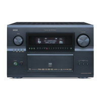
AVR-5803/AVC-A1SR
25 P84/INT2 _B. DOWN I —
E↓&L
— Eu Z — Power down detect (L: Down)
26 P83/INT1 _PROTECT I —
E↑&L
— Ed Z — Protection detect input (H: Detected)
27 P82/INT0 REMOCON I —
E↑&L
— Ed Z — Remote control signal input
28 P81 SEL A (M) I — Lv — Eu Z — Master Volume turn detect input (Rotary encoder)
29 P80 SEL B (M) I — Lv — Eu Z — Master Volume turn detect input (Rotary encoder)
30 P77 ADOVER O C — — — Z L
AD Overload detect control (For subwoofer channel, H: Overload) (5803 only)
31 P76 RSPOWER O C — — — Z L Same logic with Power Port
32 P75 V.EXP OE O C — — — Z L Port Expander control output for Video circuit (BU4094B)
33 P74 V. EXP STB O C — — — Z L Port Expander control output for Video circuit (BU4094B)
34 P73/CTS2 E2P CS/VSDA O C — — — Z L EEPROM control/Video IC (Chroma-decoder, 3D Y/C)
control terminal (5803 only)
35 P72/CLK2 E2P CLK/VSCL O C — — — Z L EEPROM control/Video IC (Chroma-decoder, 3D Y/C)
control terminal (5803 only)
36 P71/RXD2 E2P DI/C. DET I — Lv — — Z —
EEPROM control/Component signal detect port (5803 only)
37 P70/TXD2 E2P DO/V. DET O/I N — — — Z L EEPROM control/Video signal detect port (5803 only)
38 P67/TXD1 TxD O C — — — Z L Data send output to external
39VCC VCC ———————+5V
40 P66/RXD1 RxD I — Lv — — Z — Data receive input from external
41VSS VSS ———————GND
42 P65/CLK1 RESET2 O C — — — Z L Output for Sub-mcom reset
43 P64/CTS1 ACK O C — — — Z — Main/Sub-mcom comm. control terminal
44 P63/TXD0 MOSI O C — — — Z L Main/Sub-mcom comm. control terminal
45 P62/RXD0 MISO I — Lv — — Z — Main/Sub-mcom comm. control terminal
46 P61/CLK0 CLK I/O (C) — — — Z Main/Sub-mcom comm. control terminal
47 P60/CTS0 REQ I — Lv — Eu Z — Main/Sub-mcom comm. control terminal
48 P137 E2P/VOE O C — — — Z L E2P and Video control port (P70~73) switching terminal
(5803 only, UPDATE: L fixed)
49 P136 EXP CLK O C — — — Z L Expander control CLK output
50 P135 EXP DATA O C — — — Z L Expander control DATA output
51 P134 MUTE POWER O C — — — Z L Same logic with Power Port (H 30ms before POWER port
at ON, but same timing at OFF)
52 P57/RDY /RDY I — — — Eu Z — Not used (Fixed to H)
53 P56/ALE ALE O C — — — — L Not used (NC)
54 P55/HOLD /HOLD I — — — Eu Z — Not used (Fixed to H)
55 P54/HLDA /HLDA O C — — — H L Not used (NC)
56 P133 POWER O C — — — Z H Power Relay control output (H: ON)
57VSS VSS ———————GND
58 P132 SP. EXP OE O C — — — Z H
Port Expander control output for speaker output (BU4094B)
59VCC VCC ———————+5V
60 P131 FL RST O C -— — — Z H FLD control terminal (LC75711NE)
61 P130 FL CE O C — -— — Z H FLD control terminal (LC75711NE)
62 P53/BCLK BCLK O C — — — Z L Not used (NC)
63 P52/RD /RD O C — — — H L Flash ROM control terminal
64 P51/BHE /BHE O C — — — — L Not used (NC)
65 P50/WR /WR O C — — — H L Flash ROM control terminal
66 P127 PL/FL/LED DATA O C — — — Z L
PLL & FLD & LED control terminal (LC72131 & LC75711NE & M66313)
67 P126 PL/FL/LED CLK O C — — — Z L
PLL & FLD & LED control terminal (LC72131 & LC75711NE & M66313)
68 P125 PLL STB O C — — — Z L PLL control terminal (LC72131)
69 P47/CS0/A23 FLASH CE O C — — — — L Control output for Flash ROM
70 P46/CS1/A22 CS1 O C — — — — L Not used
71 P45/CS2/A21 CS2 O C — — — — L Not used
72 P44/CS3/A20 CS3 O C — — — — L Not used
73 P43/A19 NOT USED O C — — — — L Not used
74VCC VCC ———————+5V
75 P42/A18 MA17 O C — — — — L Flash ROM control terminal
76VSS VSS ———————GND
77 P41/A17 MA16 O C — — — — L Flash ROM control terminal
78 P40/A16 MA15 O C — — — — L Flash ROM control terminal
79 P37/A15 MA14 O C — — — — L Flash ROM control terminal
80 P36/A14 MA13 O C — — — — L Flash ROM control terminal
81 P35/A13 MA12 O C — — — — L Flash ROM control terminal
82 P34/A12 MA11 O C — — — — L Flash ROM control terminal
83 P33/A11 MA10 O C — — — — L Flash ROM control terminal
84 P32/A10 MA9 O C — — — — L Flash ROM control terminal
85 P31/A9 MA8 O C — — — — L Flash ROM control terminal
86 P124 E. VOL CLK O C — — — Z L E. VR control output (TC9459)
87 P123 E. VOL DATA O C — — — Z L E. VR control output (TC9459)
88 P122 E. VOL STBA O C — — — Z L E. VR control output (TC9459)
89 P121 E. VOL STBB O C — — — Z L E. VR control output (TC9459)
Function
Pin
No.
Pin Name
DetI/O Type Ext Int Res Init
Symbol
 Loading...