93
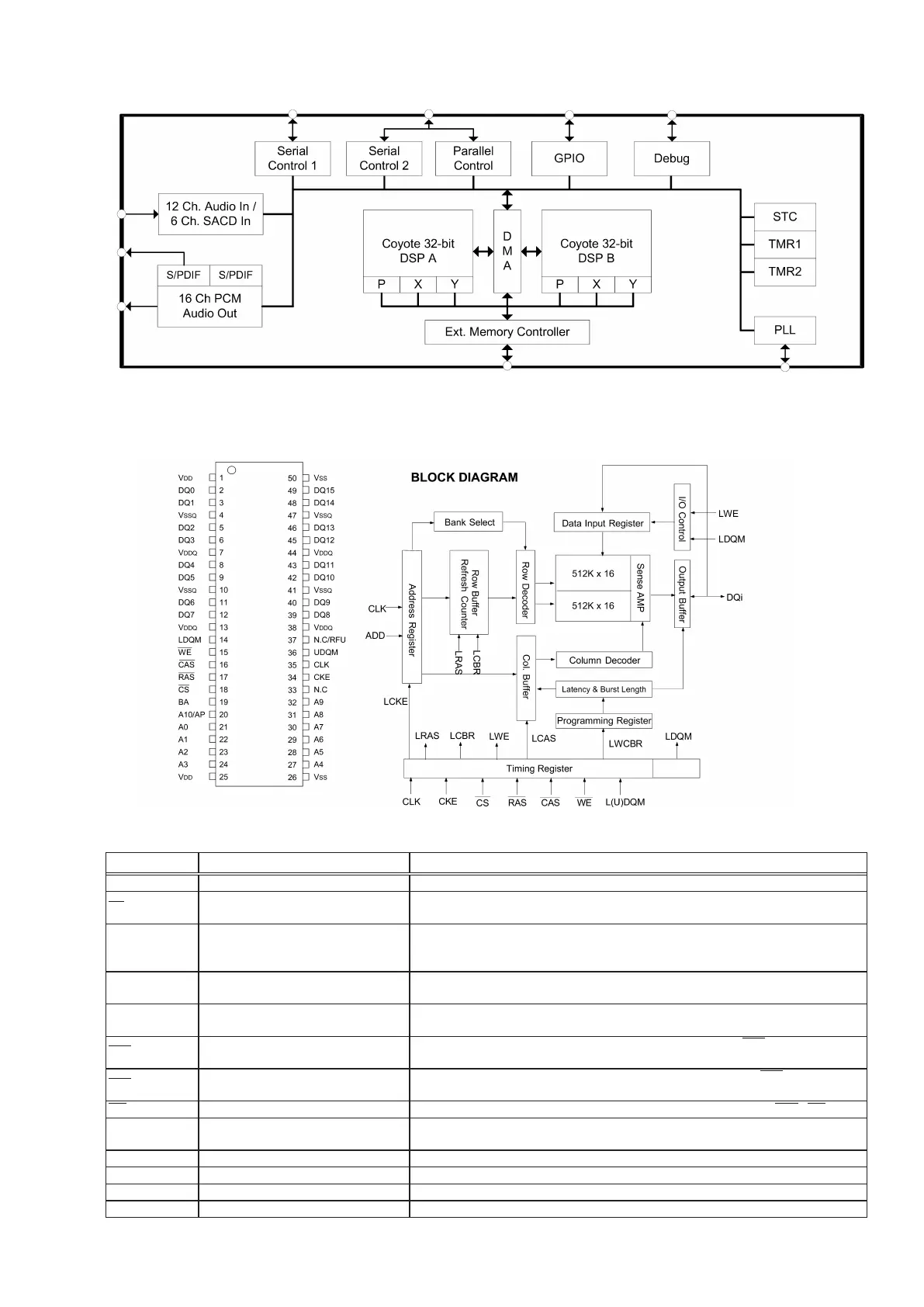
CS497024CVZ Block diagram
M12L16161A5TG (DIGITAL : IC83)
M12L16161A5TG Terminal Functions
Pin Name Input Function
CLK System Clock Active on the positive going edge to sample all inputs.
CS Chip Select
Disables or enables device operation by masking or enabling all inputs except CLK, CKE
and L(U)DQM.
CKE Clock Enable
Masks system clock to freeze operation from the next clock cycle.
CKE should be enabled at least one cycle prior to new command.
Disable input buffers for power down in standby.
A0 ~ A10/AP Address
Row / column addresses are multiplexed on the same pins.
Row address : RA0 ~ RA10, column address : CA0 ~ CA7
BA Bank Select Address
Selects bank to be activated during row address latch time. Selects bank for read/write
during column address latch time.
RAS Row Address Strobe
Latches row addresses on the positive going edge of the CLK with RAS low.
Enables row access & precharge.
CAS Column Address Strobe
Latches column addresses on the positive going edge of the CLK with CAS low.
Enables column access.
WE Write Enable Enables write operation and row precharge. Latches data in starting from CAS , WE active.
L(U)DQM Data Input / Output Mask
Makes data output Hi-Z, t
SHZ
after the clock and masks the output.
Blocks data input when L(U)DQM active.
DQ0~15 Data Input / Output Data inputs/outputs are multiplexed on the same pins.
VDD/VSS Power Supply/Ground Power and ground for the input buffers and the core logic.
VDDQ/VSSQ Data Output Power/Ground Isolated power supply and ground for the output buffers to provide improved noise immunity.
N.C/RFU No Connection/ Reserved for Future Use This pin is recommended to be left No Connection on the device.