


D
David CooperSep 8, 2025
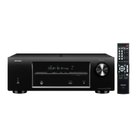
What does it mean if after turning on the power the power indicator is blinking red on Denon AVR-E200?
- AAnna StewartSep 8, 2025
If, after turning on the power, the power indicator is blinking red on your Denon Stereo Receiver, it indicates that the unit’s amplifier circuit has failed. Turn off the power and contact the Denon service advisor.