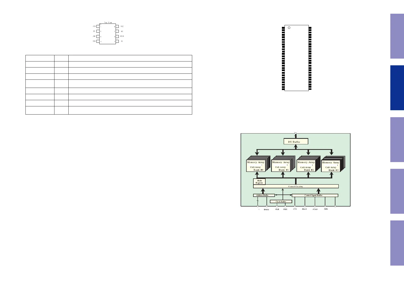
BY25D16ASSIG (DIGITAL_DSP : IC782)
Terminal Functions
1
2
3
4
8
7
6
5
Top View
SOP8 150/208mil
/CS
SO
/WP
VSS
VCC
NC
SCLK
SI
Pin Name I/O Description
/CS I Chip Select
SO (IO1) I/O Serial Output for single bit data Instructions. IO1 for Dual Instructions.
Write Protect in single bit
VSS Ground
SI (IO0) I/O Serial Input for single bit data Instructions. IO0 for Dual Instructions.
SCLK I Serial Clock
NC No Connection
VCC Core and I/O Power Supply
A3V64S40GTP-60 (DIGITAL_DSP : IC784)
Block diagram
A3V64S40GTP
64M Single Data Rate Synchronous DRAM
Revision 1.0 Dec., 2012
CLK : Master Clock U,LDQM : Output Disable / Write Mask
CKE : Clock Enable A0-11 : Address Input
/CS : Chip Select BA0,1 : Bank Address
/RAS : Row Address Strobe Vdd : Power Supply
/CAS : Column Address Strobe VddQ : Power Supply for Output
/WE : Write Enable Vss : Ground
DQ0-15 : Data I/O VssQ : Ground for Output
PIN CONFIGURATION (TOP VIEW)
A3V64S40GTP
64M Single Data Rate Synchronous DRAM
Revision 1.0 Dec., 2012
BLOCK DIAGRAM
Type Designation Code
Before Servicing
This Unit
Electrical Mechanical Repair Information Updating
48
 Loading...