M24C32WMN6TP (DIGITAL : IC712)
ADV7623 (DIGITAL : IC721)
M24128, M24C64, M24C32 Description
7/39
Figure 2. DIP, SO, TSSOP and UFDFPN connections
1. See Package mechanical data section for package dimensions, and how to identify pin-1.
Figure 3. M24128 WLCSP connections (top view, marking side, with balls on the
underside)
Table 2. Signal names
Signal name Function Direction
E0, E1, E2 Chip Enable Input
SDA Serial Data I/O
SCL Serial Clock Input
WC Write Control Input
V
CC
Supply voltage
V
SS
Ground
SDAV
SS
SCL
WCE1
E0 V
CC
E2
AI01845e
M24128
M24C64
M24C32
1
2
3
4
8
7
6
5
V
CC
E1 E0
WC
E2
SDA SCL V
SS
ai14799
ADV7623 Hardware Manual
Rev. 0 – March 2010 16 Confidential NDA required
2.7 Pin Description
DDCC_SDA
5V_DETC
HP_CTRLC
RXB_2+
RXB_2-
TVDD
RXB_1+
RXB_1-
CGND
RXB_0+
RXB_0-
TVDD
RXB_C+
RXB_C-
CGND
CVDD
DDCB_SCL
DDCB_SDA
DVDD
DGND
5V_DETB
HP_CTRLB
RXA_2+
RXA_2-
TVDD
RXA_1+
RXA_1-
CGND
RXA_0+
RXA_0-
TVDD
RXA_C+
RXA_C-
CGND
CVDD
DDCA_SCL
144
143
142
141
140
139
138
137
136
135
134
133
132
131
130
129
128
127
126
125
124
123
122
121
120
119
118
117
116
115
114
113
112
111
110
109
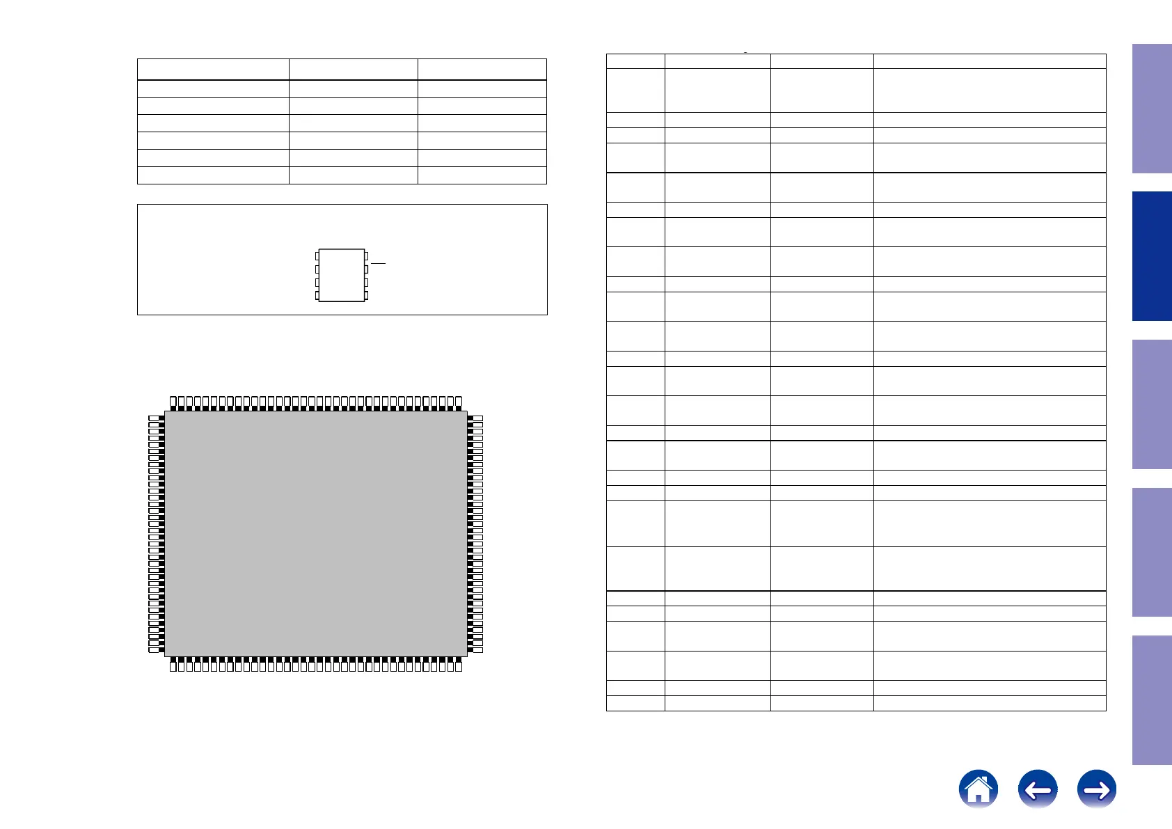
DDCC_SCL 1 108 DDCA_SDA
CVDD 2 107 RTERM
CGND 3 106 5V_DETA
RXC_C- 4 105 HP_CTRLA
RXC_C+ 5 104 PGND
TVDD 6 103 PVDD
RXC_0- 7 102 XTAL1
RXC_0+ 8 101 XTAL
CGND 9 100 PVDD
RXC_1- 10 99 PGND
RXC_1+ 11 98 PWRDNB
TVDD 12 97 RESETB
RXC_2- 13 96 MCLK_OUT
RXC_2+ 14 95 SCLK_OUT
HP_CTRLD 15 94 AP5_OUT
5V_DETD 16 93 DVDD
DGND 17 92 DGND
DVDD 18 91 AP4_OUT
DDCD_SDA 19 90 AP3_OUT
DDCD_SCL 20 89 AP2_OUT
CVDD 21 88 AP1_OUT
CGND 22 87 AP0_OUT
RXD_C- 23 86 DVDDIO
RXD_C+ 24 85 DGNDIO
TVDD 25 84 INT_TX
RXD_0- 26 83 INT2
RXD_0+ 27 82 INT1
CGND 28 81 DVDD
RXD_1- 29 80 DGND
RXD_1+ 30 79 SCL
TVDD 31 78 SDATA
RXD_2- 32 77 AP0_IN
RXD_2+ 33 76 AP1_IN
CVDD 34 75 AP2_IN
CGND 35 74 AP3_IN
TXPVDD 36 73 DVDDIO
37
38
39
40
41
42
43
44
45
46
47
48
49
50
51
52
53
54
55
56
57
58
59
60
61
62
63
64
65
66
67
68
69
70
71
72
TXPLVDD
TXPGND
TXPLGND
EXT_SWING
HPD_ARC-
ARC+
TXDDC_SD
TXDDC_SCL
TXAVDD
TXGND
TXC-
TXC+
TXGND
TX0-
TX0+
TXGND
TX1-
TX1+
TXAVDD
TX2-
TX2+
TXGND
CEC
DGND
DVDD
ALSB
CSB
EP_SCK
EP_CS
EP_MOSI
EP_MISO
MCLK_IN
SCLK_IN
AP5_IN
AP4_IN
DGNDIO
Figure 3: ADV7623 Pin Configuration
Terminal Functions
ADV7623 Hardware Manual
Rev. 0 – March 2010 17 Confidential NDA required
Table 6. Function Descriptions
Location Mnemonic Type Description
1 DDCC_SCL Digital Input HDCP slave serial clock port C.
DDCC_SCL is a 3.3 V input that is 5 V
tolerant.
2 CVDD Power Receiver comparator supply voltage (1.8V)
3 CGND Ground TVDD and CVDD Ground
4 RXC_C- HDMI Input Digital input clock Complement of port C
in the HDMI interface.
5 RXC_C+ HDMI Input Digital input clock True of port C in the
HDMI interface.
6 TVDD Power Receiver terminator supply voltage (3.3 V)
7 RXC_0- HDMI Input Digital input channel 0 Complement of port
C in the HDMI interface.
8 RXC_0+ HDMI Input Digital input channel 0 True of port C in
the HDMI interface.
9 CGND Ground TVDD and CVDD Ground
10 RXC_1- HDMI Input Digital input channel 1 Complement of port
C in the HDMI interface.
11 RXC_1+ HDMI Input Digital input channel 1 True of port C in
the HDMI interface.
12 TVDD Power Receiver terminator supply voltage (3.3 V)
13 RXC_2- HDMI Input Digital input channel 2 Complement of port
C in the HDMI interface.
14 RXC_2+ HDMI Input Digital input channel 2 True of port C in
the HDMI interface.
15 HP_CTRLD Digital Output Hot Plug Detect for Port D.
16 5V_DETD Digital Input 5 V detect pin for port D in the HDMI
interface.
17 DGND Ground Ground for DVDD
18 DVDD Power Digital supply voltage (1.8 V)
19 DDCD_SDA Digital I/O HDCP slave serial data ports D.
DDCD_SDA is a 3.3 V input/output that is
5 V tolerant.
20 DDCD_SCL Digital Input HDCP slave serial clock port D.
DDCD_SCL is a 3.3 V input that is 5 V
tolerant.
21 CVDD Power Receiver comparator supply voltage (1.8V)
22 CGND Ground TVDD and CVDD Ground
23 RXD_C- HDMI Input Digital input clock Complement of port D
in the HDMI interface.
24 RXD_C+ HDMI Input Digital input clock True of port D in the
HDMI interface.
25 TVDD Power Receiver terminator supply voltage (3.3 V)
26 RXD_0- HDMI Input Digital input channel 0 Complement of port
34
Caution in
servicing
Electrical Mechanical Repair Information Updating

 Loading...