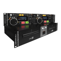
37
DN-HD2500
W9812G6GH-6 (IC104, 105, 502, 503)
M29W800DT70N1 (IC405)
PIN DESCRIPTION
PIN NUMBER
23 - 26, 22,
29 - 35
A0 - A11 Address
Multiplexed pins for row and column address.
Row address: A0 - A11. Column address: A0 - A8.
Select bank to activate during row address latch time,
or bank to read/write during address latch time.
Multiplexed pins for data output and input.
Disable or enable the command decoder. When
command decoder is disabled, new command is
ignored and previous operation continues.
Bank Select
Data Input/
Output
Chip Select
Roe Address
Strobe
Column Address
Strobe
Write Enable
Input/Output
Mask
Clock Inputs
Clock Enable
Power (+3.3V)
Power (+3.3V)
for I/O Buffer
Ground for I/O
Buffer
No Connection No Connection
Ground
BS0, BS1
DQ0 -
DQ5
20, 21
2, 4, 5, 7, 8,
10, 11, 13, 42,
44, 45, 47, 48,
50, 51, 53
19
18
17
16
39, 15
38
37
1, 14, 27
28, 41, 54
3, 9, 43, 49
6, 12, 46, 52
36, 40
PIN NAME FUNCTION DESCRIPTION
CS
UDQM/
LDQM
CLK
CKE
Vcc
Vss
VccQ
VssQ
NC
WE
RAS
CAS
Command input, When sampled at the rising edge of
the clock, RAS, CAS and WE define the operation
to be executed.
Referred to RAS
The output buffer is placed at Hi-Z (with latency of 2)
when DQM is sampled high in read cycle. In write
cycle, sampling DQM high will block the write operation
with zero latency.
System clock used to sample inputs on the rising edge
of clock.
CKE controls the clock activation and deactivation.
When CKE is low, Power Down mode, Suspend mode
or Self Refresh mode is entered.
Power for input buffers and logic circuit inside DRAM.
Ground for input buffers and logic circuit inside DRAM.
Separated power from Vcc, used for output buffers to
improve noise.
Separated power from Vss, used for output buffers to
improve noise.
Referred to RAS
1
2
3
4
5
6
7
8
9
10
11
12
13
14
15
16
17
18
19
20
21
25
24
23
22
V
CC
V
CC
Q
DQ0
V
SS
Q
DQ2
V
SS
Q
DQ6
V
CC
Q
DQ4
BS0
BS1
A10/AP
A0
DQ1
DQ5
V
CC
LDQM
Vcc
WE
CAS
RAS
CS
DQ7
DQ3
26
27
A1
A2
V
SS
VssQ
DQ15
V
CC
Q
DQ13
V
CC
Q
DQ9
V
SS
Q
DQ11
A9
A8
A7
A6
A5
DQ14
DQ10
V
SS
NC
UDQM
CLK
CKE
NC
A11
DQ8
DQ12
A4
Vss
54
53
52
51
50
49
48
47
46
45
44
43
42
41
40
39
38
37
36
35
34
30
31
32
33
29
28
A3
DQ3
DQ9
DQ2
A6
DQ0
W
A3
RB
DQ6
A8
A9
DQ13
A17
A10 DQ14
A2
DQ12
DQ10
DQ15A–1
V
CC
DQ4
DQ5
A7
DQ7
NC
NC
M29W800DT
M29W800DB
12
1
13
24 25
36
37
48
DQ8
NC
NC
A1
A18
A4
A5
DQ1
DQ11
G
A12
A13
A16
A11
BYTE
A15
A14
V
SS
E
A0
RP
V
SS
Logic Diagram Signal Names
AI05470B
19
A0-A18
W
DQ0-DQ14
V
CC
M29W800DT
M29W800DB
E
V
SS
15
G
RP
DQ15A–1
RB
BYTE
A0-A18 Address Inputs
DQ0-DQ7 Data Inputs/Outputs
DQ8-DQ14 Data Inputs/Outputs
DQ15A–1 Data Input/Output or Address Input
E
Chip Enable
G
Output Enable
W
Write Enable
RP
Reset/Block Temporary Unprotect
RB
Ready/Busy Output
(not available on SO44 package)
BYTE
Byte/Word Organization Select
V
CC
Supply Voltage
V
SS
Ground
NC Not Connected Internally
 Loading...