42
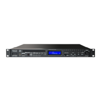
DN-S1200
69 TxD2 TX O SCIF Tx Memo Terminal (Memo Link Tx)
70 PE9 PE9 O General-purpose port OPEN
71 PE10 PE10 O General-purpose port OPEN
72 PE11 PE11 O General-purpose port OPEN
73 RxD3 PS2RX I SCIF Rx AVR UART Terminal
74 VCC VCC P Power supply for in Digital +1.2V
75 PC14 USB_H/D O General-purpose port USB_A/B switching SW(H=Host, L=Device)
76 VSS VSS G Digital GND
77 PVSS PVSS G GND for I/O Digital GND
78 RTC_X1 RTC_X1 I Empty pin processing Unused: GND
79 RTC_X2 RTC_X2 O Empty pin processing Unused: OPEN
80 PVCC PVCC P Power supply for I/O Digital +3.3V
81 TX3 PS2TX O SCIF Tx AVR UART Terminal
82 PE14 PS2RST O General-purpose port AVR Reset Terminal
83 PE15 BOOTCLK O General-purpose port AVR writing CLK
84 PVSS PVSS G GND for I/O Digital GND
85 PB8 CD_RST O General-purpose port
Serbo DSP Reset signal output(Active=L)
Pull Down
86 PB9 SUBDATA I General-purpose port Serbo DSP subcord data input
87 PB10 PB10 I General-purpose port OPEN
88 PB11 SUBCK O General-purpose port Serbo DSP subcord clock output
89 VCC VCC P Power supply for in Digital +1.2V
90 MD MD I
Mode setting
(1:32bit/0:16bit)
Pull-down in GND
91 VSS VSS G Digital GND
92 PVSS PVSS G GND for I/O Digital GND
93 USB_X1 USB_X1 Clock generation for USB 48MHz X 'tal connection
94 USB_X2 USB_X2
↑↑
95 PVCC PVCC P Power supply for I/O Digital +3.3V
96 MD_CLK1 MD_CLK1 I Clock selection setting
97 MD_CLK0 MD_CLK0 I
↑
98 USBDPVSS USBDPVSS G Digital GND for drive Digital GND
99 USBDPVCC USBDPVCC P
Digital power supply for driver
Digital +3.3V
100 DM DM I/O D-terminal USB connector connection
101 DP DP I/O D + terminal
↑
102 VBUS VBUS I VBUS detection terminal
TerminalVBUSconnectingdirectly
through56Ω
103 USBAVCC USBAVCC P
Analog power supply
for in driver
Analogue +1.2V
104 USBAVSS USBAVSS G Analog GND for in driver Analog GND
105 REFRIN REFRIN I
Reference resistance
connection
ConnectsitGNDby5.6kΩ ± 1%resistance
106 USBAPVSS USBAPVSS G Analog GND for driver Analog GND
107 USBAPVCC USBAPVCC P
Analog power supply
for driver
Analogue +3.3V
108 USBDVCC USBDVCC P
Digital power supply
for in driver
Digital +1.2V
109 USBDVSS USBDVSS G Digital GND for in driver Digital GND
110 AN0 PITCH1 I ADC input Deck1 Pitch input
111 AN1 CENT1 I ADC input Deck1 Center input
112 AN2 AN2 I ADC input GND
113 AN3 AN3 I ADC input GND
114 AVCC AVCC P Power supply for ADC/DAC After LC, +3.3V is supplied
115 AN4 AN4 I ADC input GND
116 AVREF AVREF I
Conversion standard voltage
114pin and connection
117 AN5 TEST1 I ADC input
Serbo DSPTEST1 input
(automatic adjusting abnormal condition=H)
118 DA0 LOADING O DAC output CD Loading Motor DAC output (default:80h)
119 DA1 LED1 O DAC output OPEN
120 AVSS AVSS G GND for ADC/DAC Analog GND
121 PVSS PVSS G GND for I/O Digital GND
122 /WDTOVF /WDTOVF O WDT output(L active) OPEN
123 PVCC PVCC P Power supply for I/O Digital +3.3V
124 PF29 PF29 O General-purpose port OPEN
125 PF28 PF28 O General-purpose port OPEN
126 PF27 PF27 O General-purpose port OPEN
127 VCC VCC P Power supply for in Digital +1.2V
128 PF30 PF30 O General-purpose port OPEN
129 VSS VSS G Digital GND
130 PVSS PVSS G GND for I/O Digital GND
131 AUDIO_X1 AUDIO_X1 I Not used GND
132 AUDIO_X2 AUDIO_X2 O Not used OPEN
133 PVCC PVCC P Power supply for I/O Digital +3.3V
134 PF26 PF26 O General-purpose port OPEN
Pin No. Pin Name Symble I/O Function

 Loading...