TPS2065CDBVR(IC1301)
TPS2065CDBVRBlockDiagram
TPS2065CDBVRPinDiscriptions
GND
IN
IN
EN or EN
OUT
OUT
OUT
FLT
1
2
3
4 5
6
7
8
GND
OUT
FLT
IN
1
2
3
5
4
(Top V iew)
EN or EN
OUT
IN
GND
FLT
R
FLT
10 k
Control Signal
V
IN
0.1 F
150 F
Fault Signal
Pad*
V
OUT
* DGN only
EN or
EN
TPS20xxC
www.ti.com
SLVSAU6A – JUNE 2011 – REVISED JULY 2011
Current-Limited, Power-Distribution Switches
Check for Samples: TPS20xxC
1
FEATURES DESCRIPTION
The TPS20xxC power-distribution switch family is
23
• Single Power Switch Family
intended for applications such as USB where heavy
• Pin for Pin with Existing TI Switch Portfolio
capacitive loads and short-circuits are likely to be
• Rated currents of 0.5 A, 1 A, 1.5 A, 2 A
encountered. This family offers multiple devices with
fixed current-limit thresholds for applications between
•±20% Accurate, Fixed, Constant Current Limit
0.5 A and 2 A.
• Fast Over-Current Response – 2 µs
The TPS20xxC family limits the output current to a
• Deglitched Fault Reporting
safe level by operating in a constant-current mode
• Output Discharge When Disabled
when the output load exceeds the current-limit
• Reverse Current Blocking
threshold. This provides a predictable fault current
under all conditions. The fast overload response time
• Built-in Softstart
eases the burden on the main 5 V supply to provide
• Ambient Temperature Range: –40°C to 85°C
regulated power when the output is shorted. The
power-switch rise and fall times are controlled to
APPLICATIONS
minimize current surges during turn-on and turn-off.
• USB Ports/Hubs, Laptops, Desktops
• High-Definition Digital TVs
• Set Top Boxes
• Short-Circuit Protection
TYPICAL APPLICATION
Figure 1. Typical Application
Table 1. DEVICES
(1)
STATUS
MAXIMUM OPERATING
DEVICES
MSOP-8
CURRENT
SOT23-5
(PowerPad) ™
0.5 TPS2051C - Preview
1 TPS2065C Active Preview
1.5 TPS2069C Active -
2 TPS2000C / 1C Active -
(1) For more details, see the DEVICE INFORMATION table.
1
Please be aware that an important notice concerning availability, standard warranty, and use in critical applications of Texas
Instruments semiconductor products and disclaimers thereto appears at the end of this data sheet.
2PowerPAD is a trademark of Texas Instruments.
3 is a trademark of ~ Texas Instruments.
UNLESS OTHERWISE NOTED this document contains
Copyright © 2011, Texas Instruments Incorporated
PRODUCTION DATA information current as of publication date.
Products conform to specifications per the terms of Texas
Instruments standard warranty. Production processing does not
necessarily include testing of all parameters.
Charge
Pump
Driver
UVLO
Current
Limit
Thermal
Sense
9-ms
Deglitch
IN
GND
FLT
Sense
(Disabled+
UVLO)
OTSD
CS
N
TPS20xxC
SLVSAU6A – JUNE 2011 – REVISED JULY 2011
www.ti.com
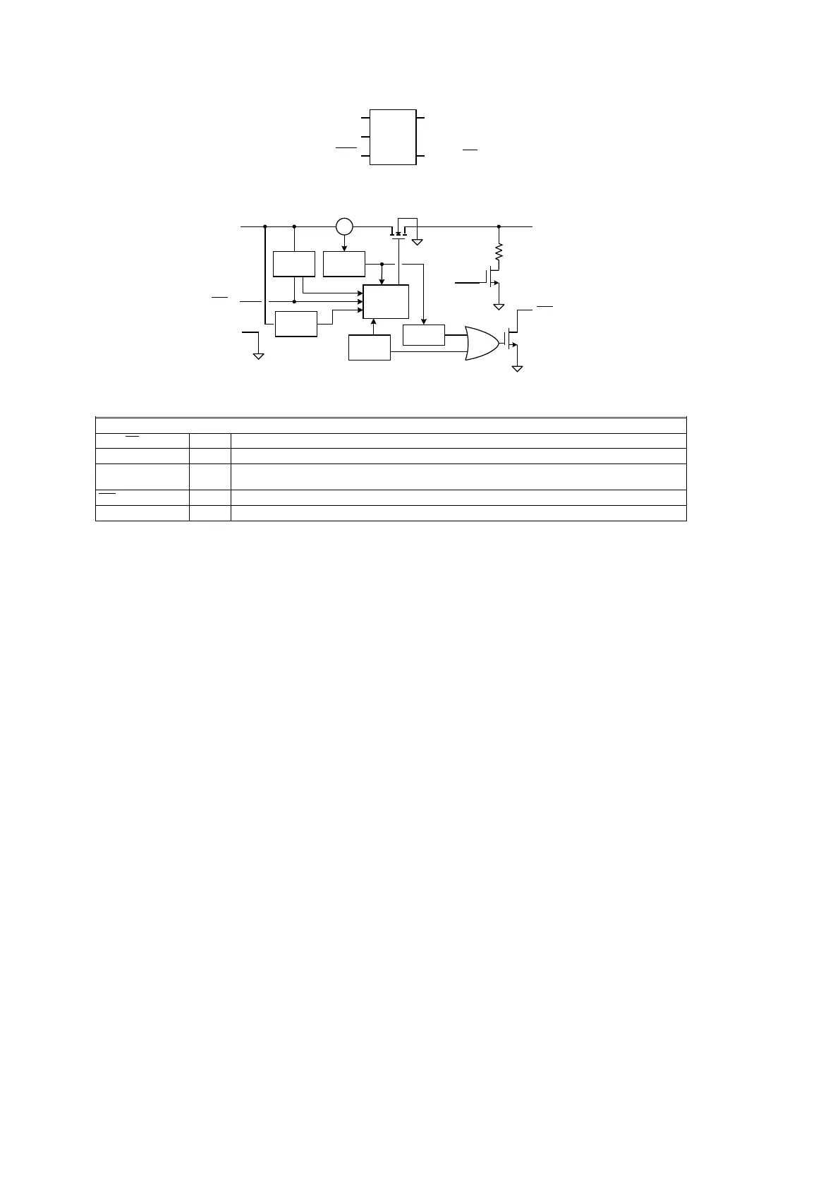
FUNCTIONAL BLOCK DIAGRAM
DEVICE INFORMATION
PIN FUNCTIONS
NAME PINS DESCRIPTION
8-PIN PACKAGE
EN or EN 4 Enable input, logic high turns on power switch
GND 1 Ground connection
IN 2, 3 Input voltage and power-switch drain; connect a 0.1 µF or greater ceramic capacitor from IN to GND close
to the IC
FLT 5 Active-low open-drain output, asserted during over-current, or over-temperature conditions
OUT 6, 7, 8 Power-switch output, connect to load
PowerPAD PAD Internally connected to GND. Connect PAD to GND plane as a heatsink for the best thermal performance.
(DGN ONLY) PAD may be left floating if desired. See POWER DISSIPATION AND JUNCTION TEMPERATURE section
for guidance.
5-PIN PACKAGE
EN or EN 4 Enable input, logic high turns on power switch
GND 2 Ground connection
IN 5 Input voltage and power-switch drain; connect a 0.1 µF or greater ceramic capacitor from IN to GND close
to the IC
FLT 3 Active-low open-drain output, asserted during over-current, or over-temperature conditions
OUT 1 Power-switch output, connect to load.
6
Copyright © 2011, Texas Instruments Incorporated
Charge
Pump
Driver
UVLO
Current
Limit
Thermal
Sense
9-ms
Deglitch
IN
GND
OUT
FLT
Current
Sense
(Disabled+
UVLO)
OTSD
CS
EN or
EN
TPS20xxC
SLVSAU6A – JUNE 2011 –REVISED JULY 2011
www.ti.com
FUNCTIONAL BLOCK DIAGRAM
DEVICE INFORMATION
PIN FUNCTIONS
NAME PINS DESCRIPTION
8-PIN PACKAGE
EN or EN 4 Enable input, logic high turns on power switch
GND 1 Ground connection
IN 2, 3 Input voltage and power-switch drain; connect a 0.1 µF or greater ceramic capacitor from IN to GND close
to the IC
FLT 5 Active-low open-drain output, asserted during over-current, or over-temperature conditions
OUT 6, 7, 8 Power-switch output, connect to load
PowerPAD PAD Internally connected to GND. Connect PAD to GND plane as a heatsink for the best thermal performance.
(DGN ONLY) PAD may be left floating if desired. See POWER DISSIPATION AND JUNCTION TEMPERATURE section
for guidance.
5-PIN PACKAGE
EN or EN 4 Enable input, logic high turns on power switch
GND 2 Ground connection
IN 5 Input voltage and power-switch drain; connect a 0.1 µF or greater ceramic capacitor from IN to GND close
to the IC
FLT 3 Active-low open-drain output, asserted during over-current, or over-temperature conditions
OUT 1 Power-switch output, connect to load.
6 Copyright © 2011, Texas Instruments Incorporated
76

 Loading...