EasyManua.ls Logo

Denon DRA-100 Service Manual

Denon DRA-100
98 pages
To Next Page IconTo Next Page
Page #1 background imageLoading...
Page #1 background image
MODEL JP E3 E2 EK EA E1 E1C E1K
DRA-100
P P
NETWORK RECEIVER
S1222V03DM/DG1603
Ver. 3
Please use this service manual with referring to the operating instructions without fail.
Some illustrations using in this service manual are slightly different from the actual set.
• For purposes of improvement, specications and design are subject to change without notice.
Please refer to the
MODIFICATION NOTICE.
e
SERVICE MANUAL
e
D&M Holdings Inc.
Copyright 2016 D&M Holdings Inc. All rights reserved.
WARNING: Violators will be prosecuted to the maximum extent possible.

Other manuals for Denon DRA-100

Question and Answer IconNeed help?

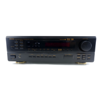
Do you have a question about the Denon DRA-100 and is the answer not in the manual?

Denon DRA-100 Specifications

General IconGeneral
Internet radioYes
Supported radio bands-
Impedance8 Ω
RMS rated power70 W
Product colorSilver
Headphone connectivity6.3 mm
AUX inNo
Audio (L/R) out1
AC outlets quantity1 AC outlet(s)
Power consumption (typical)60 W
Weight and Dimensions IconWeight and Dimensions
Depth332 mm
Width280 mm
Height160 mm
Weight4800 g
Dimensions (WxDxH)280 x 332 x 160 mm

Summary

Using Adobe Reader Features

Magnifying Diagrams (Ctrl+Space)

Details on magnifying diagrams using Ctrl+Space and mouse drag.

Advanced Adobe Reader Diagram Tools

Pan & Zoom Function for Diagrams

Explains using the Pan & Zoom function for viewing magnified diagram parts.

Loupe Tool Function for Diagrams

Describes the Loupe Tool function for magnifying specific diagram sections.

Critical Safety Precautions

Leakage Current Check Procedure

Procedure to check leakage current before returning the set to the customer.

Servicing and Inspection Cautions

General Handling and Servicing Cautions

General cautions regarding handling and servicing the unit.

Electric Shock Hazard Warnings

Warnings and precautions related to electric shock hazards.

Use of Designated Replacement Parts

Emphasizes using only specified replacement parts for safety.

Post-Servicing Safety Checks

Checklist for safety checks after completing servicing or repairs.

Important Safety Parts Identification

Highlights parts with critical safety properties requiring specific part numbers.

Handling Electrostatic Sensitive Components

Grounding Human Body for ESD Protection

Guidelines for grounding human body to prevent electrostatic discharge.

Grounding Workbench for ESD Protection

Instructions for grounding the workbench to prevent electrostatic discharge.

Technical Specifications Overview

Audio Section Specifications

Detailed specifications for the audio output, power, input sensitivity, and tone control.

Servicing Cautions and Unit Initialization

Initializing the Unit After Component Replacement

Steps to initialize the unit after replacing components like microcomputer or PCBs.

Disassembly Procedures Overview

Main PCB Assembly Disassembly

Details on disassembling the Main PCB assembly and its reference number.

Main PCB Removal Procedure

SMPS PCB Removal Procedure

Front Assembly Disassembly Steps

Bottom Assembly Removal Steps

Special Operating Modes

Accessing Special Modes via Buttons

Explains how to enter various special modes using buttons on the unit.

Factory Initialization Mode Procedure

User Initialization Mode Procedure

Post-Component Replacement Procedures

Printed Circuit Board Replacement Steps

Steps required after replacing PCBs, including region setting and software updates.

Microprocessor and Related Component Replacement

Steps after replacing the u-COM, flash ROM, or other related components.

Firmware Update Procedures

Updating Firmware via USB

Guide on downloading and updating firmware using a USB memory device.

USB Firmware Update Details

Inserting USB Memory and Starting Update

Steps for inserting USB memory and initiating the firmware update process.

Advanced Firmware Update Modes

Forced USB All Device Write Mode

Mode used for unit recovery, forcing it into USB update mode.

Update Procedure for CY920 Error

Specific update steps to resolve a "CY920 Error" displayed on the unit.

Network Firmware Update Procedures

Updating Firmware via DPMS

Guide to updating firmware over the network using the DPMS server.

Checking and Performing DPMS Firmware Update

Steps to check for available firmware updates and initiate the DPMS update.

Touch Sensor Firmware Update

Updating Touch Sensor Firmware via Unit

Procedure for updating the touch sensor firmware installed in the unit.

Starting and Monitoring Touch Sensor Update

Steps to initiate and monitor the touch sensor firmware update.

Troubleshooting: OLED Display Issues

Troubleshooting: No Sound or Noise Issues

DIR-SPK Output and Signal Troubleshooting

Troubleshooting audio issues related to DIR-SPK output and signals.

DIR-SPK Signal Path Troubleshooting

DIR-SPK Power and Control Signal Issues

Troubleshooting audio issues related to DIR-SPK power and control signals.

Preout and Subwoofer Output Troubleshooting

Analog Input Troubleshooting

Connectivity Troubleshooting (USB, Ethernet, Wi-Fi, Bluetooth)

Optical and Coaxial Input Troubleshooting

Signal Measurement and Waveform Analysis

System Block Diagram Overview

Power Distribution Diagram

Internal Wiring Diagram

Main PCB Layout Diagrams

Other PCB Layout Diagrams

Schematic Diagrams - Part 1

Schematic Diagrams - Part 2

Schematic Diagrams - Part 3

Schematic Diagrams - Part 4

SCH04 Main PCB Power Schematic

Schematic diagram detailing the power supply sections on the MAIN PCB.

Schematic Diagrams - Part 5

SCH05 Main PCB CPU and CY920 Schematic

Schematic diagram for the MAIN PCB's CPU and CY920 sections.

Schematic Diagrams - Part 6

SCH06 Main PCB DSP, DIR, FPGA Schematic

Schematic diagram for the MAIN PCB's DSP, DIR, and FPGA sections.

Schematic Diagrams - Part 7

Schematic Diagrams - Part 8

SCH08 Main PCB Speaker Output Schematic

Schematic diagram for the MAIN PCB's speaker output sections.

Schematic Diagrams - Part 9

SCH09 Main PCB Preout and Subwoofer Schematic

Schematic diagram for the MAIN PCB's preout and subwoofer output sections.

Schematic Diagrams - Part 10

SCH10 SMPS Schematic

Schematic diagram for the SMPS (Switch Mode Power Supply) section.

Semiconductor Component Details

IC Pin Assignments and Functions (IC1201)

IC Pin Assignments and Functions (IC1201) (Continued)

FPGA IC1501 Component Details

FPGA IC1501 Terminal Functions (Continued)

ADSP IC1401 Component Details

PCM9211 IC1451 Details

PCM9211 Pin Descriptions and Functions

CSRA6600 IC1601 Component Details

CSRA6600 IC1601 Terminal Functions (Continued)

CSRA6601 IC1701 Component Details

CSRA6601 IC1701 Pin Functions (Part 1)

CSRA6601 IC1701 Pin Functions (Part 2)

CSRA6601 IC1701 Pin Functions (Part 3)

CSRA6601 IC1701 Terminal Functions (Continued)

MX25L25635FMI IC1304 Details

BD11600NUX IC1302 Component Details

TPS2065CDBVR IC1301 Component Details

FL6300A SMPS IC821, IC831 Details

ICE3BR1765J SMPS IC871 Component Details

CY8C20234 IC301 Component Details

TPS562200 ICs Component Details

IP5900 IC1004 Component Details

NJM2387 IC1005 Component Details

AP7361-ADJ Voltage Regulators Component Details

NJM2752_J IC1101 Component Details

Display Component Pin Assignments