FL6300A(SMPS:IC821,IC831)
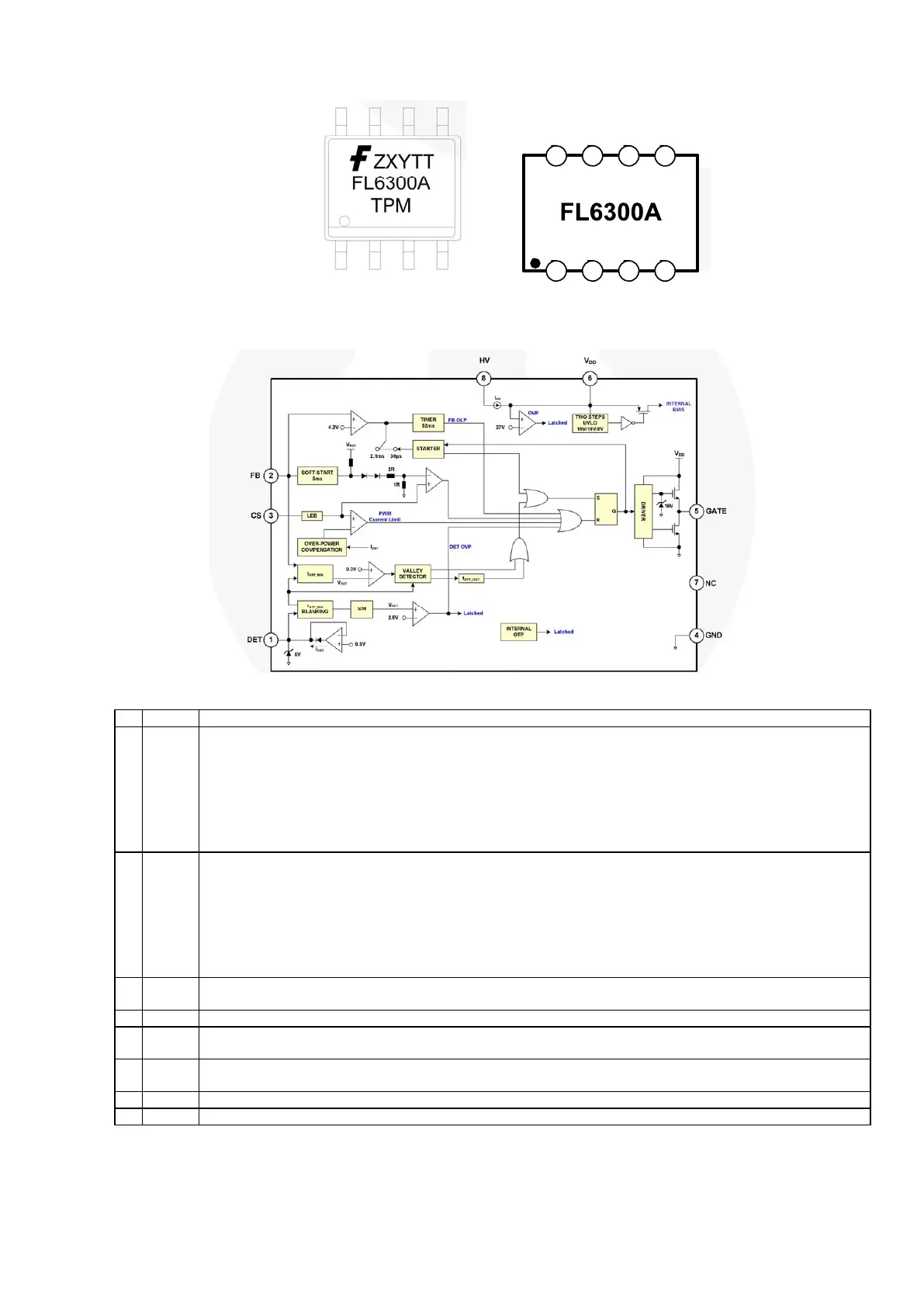
FL6300ABlockDiagram
FL6300APinDiscriptions
Pin Symbol Function
1 DET This pin is connected to an auxiliary winding of the transformer via resistors of the divider for the following purposes:
- Generates a zero-current detection (ZCD) signal once the secondary-side switching current falls to zero.
- Produces an offset voltage to compensate the threshold voltage of the peak current limit to provide a constant power
limit. The offset is generated in accordance with the input voltage when PWM signal is enabled.
- Detects the valley voltage of the switching waveform to achieve the valley voltage switching and minimize the
switching losses.
A voltage comparator and a 2.5 V reference voltage develop an output OVP protection. The ratio of the divider
determines what output voltage to stop gate, as an optical coupler and secondary shunt regulator are used.
2 FB The feedback pin should to be connected to the output of the error amplier for achieving the voltage control loop. The
FB pin should be connected to the output of the optical coupler if the error amplier is equipped at the secondary-side
of the power converter.
For primary-side control applications, FB is applied to connect a RC network to the ground for feedback-loop
compensation.
The input impedance of this pin is a 5 k equivalent resistance. A one-third (1/3) attenuator connected between the FB
and the PWM circuit is used for the loop-gain attenuation. FL6300A performs an open-loop protection (OLP) once the FB
voltage is higher than a threshold voltage (around 4.2 V) for more than 55ms.
3 CS Input to the comparator of the over-current protection. A resistor senses the switching current and the resulting voltage
is applied to this pin for the cycle-by-cycle current limit.
4 GND The power ground and signal ground. A 0.1 μF decoupling capacitor placed between VDD and GND is recommended.
5 GATE Totem-pole output generates the PWM signal to drive the external power MOSFET. The clamped gate output voltage is
18 V.
6 VDD Power supply. The threshold voltages for startup and turn-off are 16 V and 10 V, respectively.
The startup current is less than 20 μA and the operating current is lower than 4.5 mA.
7 NC No connect.
8 HV High-voltage startup.
© 2010 Fairchild Semiconductor Corporation www.fairchildsemi.com
FL6300A Rev. 1.0.2 2
Application Diagram
Figure 3. Marking Diagram
© 2010 Fairchild Semiconductor Corporation www.fairchildsemi.com
FL6300A Rev. 1.0.2 3
Pin Configuration
GND
DET
NC
CS
V
DD
1
2
3
4
8
7
6
5
FB
GATE
HV
Figure 4. Pin Assignments
Pin Definitions
Pin # Name Description
1 DET
This pin is connected to an auxiliary winding of the transformer via resistors of the divider for the
following purposes:
- Generates a zero-current detection (ZCD) signal once the secondary-side switching current
falls to zero.
- Produces an offset voltage to compensate the threshold voltage of the peak current limit to
provide a constant power limit. The offset is generated in accordance with the input voltage
when PWM signal is enabled.
- Detects the valley voltage of the switching waveform to achieve the valley voltage switching
and minimize the switching losses.
A voltage comparator and a 2.5 V reference voltage develop an output OVP protection. The
ratio of the divider determines what output voltage to stop gate, as an optical coupler and
secondary shunt regulator are used.
2 FB
The feedback pin should to be connected to the output of the error amplifier for achieving the
voltage control loop. The FB pin should be connected to the output of the optical coupler if the
error amplifier is equipped at the secondary-side of the power converter.
For primary-side control applications, FB is applied to connect a RC network to the ground for
feedback-loop compensation.
The input impedance of this pin is a 5 k
equivalent resistance. A one-third (1/3) attenuator
connected between the FB and the PWM circuit is used for the loop-gain attenuation. FL6300A
performs an open-loop protection (OLP) once the FB voltage is higher than a threshold voltage
(around 4.2 V) for more than 55ms.
3 CS
Input to the comparator of the over-current protection. A resistor senses the switching current
and the resulting voltage is applied to this pin for the cycle-by-cycle current limit.
4 GND
The power ground and signal ground. A 0.1 µF decoupling capacitor placed between V
DD
and
GND is recommended.
5 GATE
Totem-pole output generates the PWM signal to drive the external power MOSFET. The
clamped gate output voltage is 18 V.
6 V
DD
Power supply. The threshold voltages for startup and turn-off are 16 V and 10 V, respectively.
The startup current is less than 20 µA and the operating current is lower than 4.5 mA.
7 NC No connect
8 HV High-voltage startup
© 2010 Fairchild Semiconductor Corporation www.fairchildsemi.com
FL6300A Rev. 1.0.2 2
Application Diagram
Figure 3. Marking Diagram
77

 Loading...