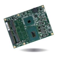
www.dfi .comChapter 3 Hardware Installation
19
Chapter 3
USB2+ A43 USB Port 2, data + or D+
USB2- A42 USB Port 2, data - or D-
USB3+ B43 USB Port 3, data + or D+
USB3- B42 USB Port 3, data - or D-
USB4+ A40 USB Port 4, data + or D+
USB4- A39 USB Port 4, data - or D-
USB5+ B40 USB Port 5, data + or D+
USB5- B39 USB Port 5, data - or D-
USB6+ A37 USB Port 6, data + or D+
USB6- A36 USB Port 6, data - or D-
USB7+ B37 USB Port 7, data + or D+
USB7- B36 USB Port 7, data - or D-
USB_0_1_OC# B44 I CMOS 3.3V Suspend/3.3V
PU 10K: to 3.3V
Suspend
USB over-current sense, USB channels 0 and 1. A pull-up for this line
shall be present on the Module. An open drain driver from a USB
current monitor on the Carrier Board may drive this line low. Do not
pull this line high on the Carrier Board.
USB over-current sense, USB ports 0 and 1.
USB_2_3_OC# A44 I CMOS 3.3V Suspend/3.3V
PU 10K: to 3.3V
Suspend
USB over-current sense, USB channels 2 and 3. A pull-up for this line
shall be present on the Module. An open drain driver from a USB
current monitor on the Carrier Board may drive this line low. Do not
pull this line high on the Carrier Board.
USB over-current sense, USB ports 2 and 3.
USB_4_5_OC# B38 I CMOS 3.3V Suspend/3.3V
PU 10K: to 3.3V
Suspend
USB over-current sense, USB channels 4 and 5. A pull-up for this line
shall be present on the Module. An open drain driver from a USB
current monitor on the Carrier Board may drive this line low. Do not
pull this line high on the Carrier Board.
USB over-current sense, USB ports 4 and 5.
USB_6_7_OC# A38 I CMOS 3.3V Suspend/3.3V
PU 10K: to 3.3V
Suspend
USB over-current sense, USB channels 6 and 7. A pull-up for this line
shall be present on the Module. An open drain driver from a USB
current monitor on the Carrier Board may drive this line low. Do not
pull this line high on the Carrier Board.
USB over-current sense, USB ports 6 and 7.
USB_SSTX0+ D4 AC Coupling capacitor USB Port 0, SuperSpeed TX +
USB_SSTX0- D3 AC Coupling capacitor USB Port 0, SuperSpeed TX -
USB_SSRX0+ C4 USB Port 0, SuperSpeed RX +
USB_SSRX0- C3 USB Port 0, SuperSpeed RX -
USB_SSTX1+ D7 AC Coupling capacitor USB Port 1, SuperSpeed TX +
USB_SSTX1- D6 AC Coupling capacitor USB Port 1, SuperSpeed TX -
USB_SSRX1+ C7 USB Port 1, SuperSpeed RX +
USB_SSRX1- C6 USB Port 1, SuperSpeed RX -
USB_SSTX2+ D10 AC Coupling capacitor USB Port 2, SuperSpeed TX +
USB_SSTX2- D9 AC Coupling capacitor USB Port 2, SuperSpeed TX -
O PCIE AC coupled on Module
Additional receive signal differential pairs for the SuperSpeed USB data
path.
I/O USB 3.3V Suspend/3.3V USB differential pairs, channel 2
Additional transmit signal differential pairs for the SuperSpeed USB data
path.
O PCIE AC coupled on Module
Additional transmit signal differential pairs for the SuperSpeed USB data
path.
I PCIE AC coupled off Module
O PCIE AC coupled on Module
Additional transmit signal differential pairs for the SuperSpeed USB data
path.
I/O USB 3.3V Suspend/3.3V USB differential pairs, channel 6
Additional receive signal differential pairs for the SuperSpeed USB data
path.
I PCIE AC coupled off Module
I/O USB 3.3V Suspend/3.3V USB differential pairs, channel 5
I/O USB 3.3V Suspend/3.3V
USB differential pairs, channel 7.
USB7 may be configured as a USB client or as a host, or both, at the
Module designer's discretion. (CH960 default set as a host)
3.3V Suspend/3.3V USB differential pairs, channel 4
I/O USB 3.3V Suspend/3.3V USB differential pairs, channel 3
I/O USB
Signal Pin# Pin Type Pwr Rail /Tolerance CH960 PU/PD Module Base Specification R2.1 Description COM Express Carrier Design Guide R2.0 Description
USB Si