User Manual V3.1
Element14 | element14.com/minode 7
Connects to a micro:bit pin with analog input or PWM function
Connects to a micro:bit pin with analog input or PWM function
Connects to a micro:bit pin with analog input or PWM function
b) Digital IO
Connects to a micro:bit pin with digital IO (input or output) function
Connects to a micro:bit pin with digital IO (input or output) function
Connects to a micro:bit pin with digital IO (input or output) function
Connects to a micro:bit pin with digital IO (input or output) function
c) I2C (Inter-Integrated Circuit)
This is a form of electronic communication standard that requires two signals, a data
signal and a clock signal. It allows information to be sent in packages, on what is called a
bus, to and from the BBC micro:bit and any attached sensor modules.
It also allows you to communicate to several sensor modules using the same bus. This is
done by identifying each sensor module with a different address.
I2C clock signal. Connect to micro:bit pin19
I2C data signal. Connect to micro:bit pin20
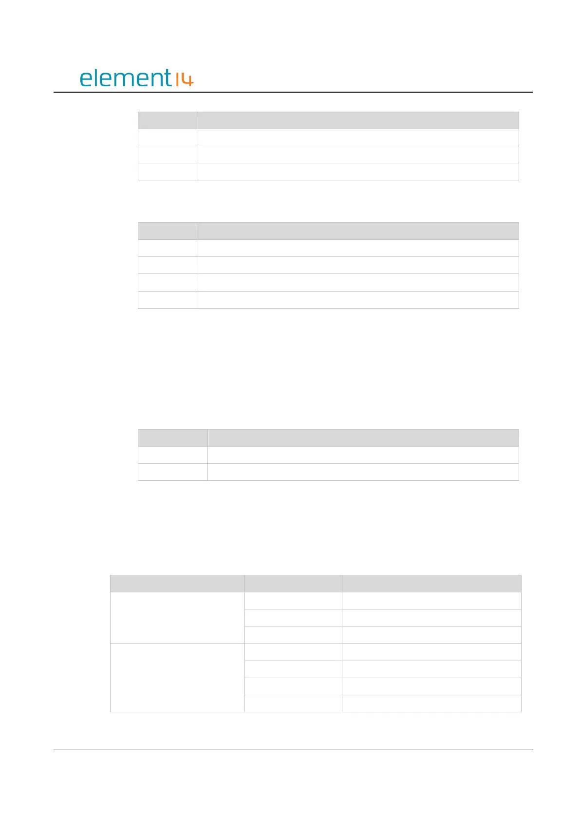
2.4 Pin Mapping
Pin mapping is done to ensure the outputs from the mi:node E-Connector pins are correctly
connected (or ‘mapped’) to the corresponding pins of the BBC micro:bit edge-connector. Below
is a table illustrating the mi:node Pin Mapping.
Analog Input / Digital IO