29
• 8 Banks
• Programmable CAS Latency(posted CAS): 5,6,7,8,9,10,11,13
• Programmable Additive Latency: 0, CL-2 or CL-1 clock
• Programmable CAS Write Latency (CWL) = 5 (DDR3-800), 6 (DDR3-1066), 7 (DDR3-
1333), 8 (DDR3-1600) and 9 (DDR3-1866)
• 8-bit pre-fetch
• Burst Length: 8 (Interleave without any limit, sequential with starting address “000” only), 4
with tCCD = 4 which does not allow seamless read or write [either On the fly using A12 or
MRS]
• Bi-directional Differential Data-Strobe
• Internal(self) calibration : Internal self calibration through ZQ pin (RZQ : 240 ohm ± 1%)
• On Die Termination using ODT pin
• Average Refresh Period 7.8us at lower than TCASE 85°C, 3.9us at 85°C < TCASE < 95 °C
• Asynchronous Reset
• Package : 78 balls FBGA - x4/x8
• All of Lead-Free products are compliant for RoHS
• All of products are Halogen-free
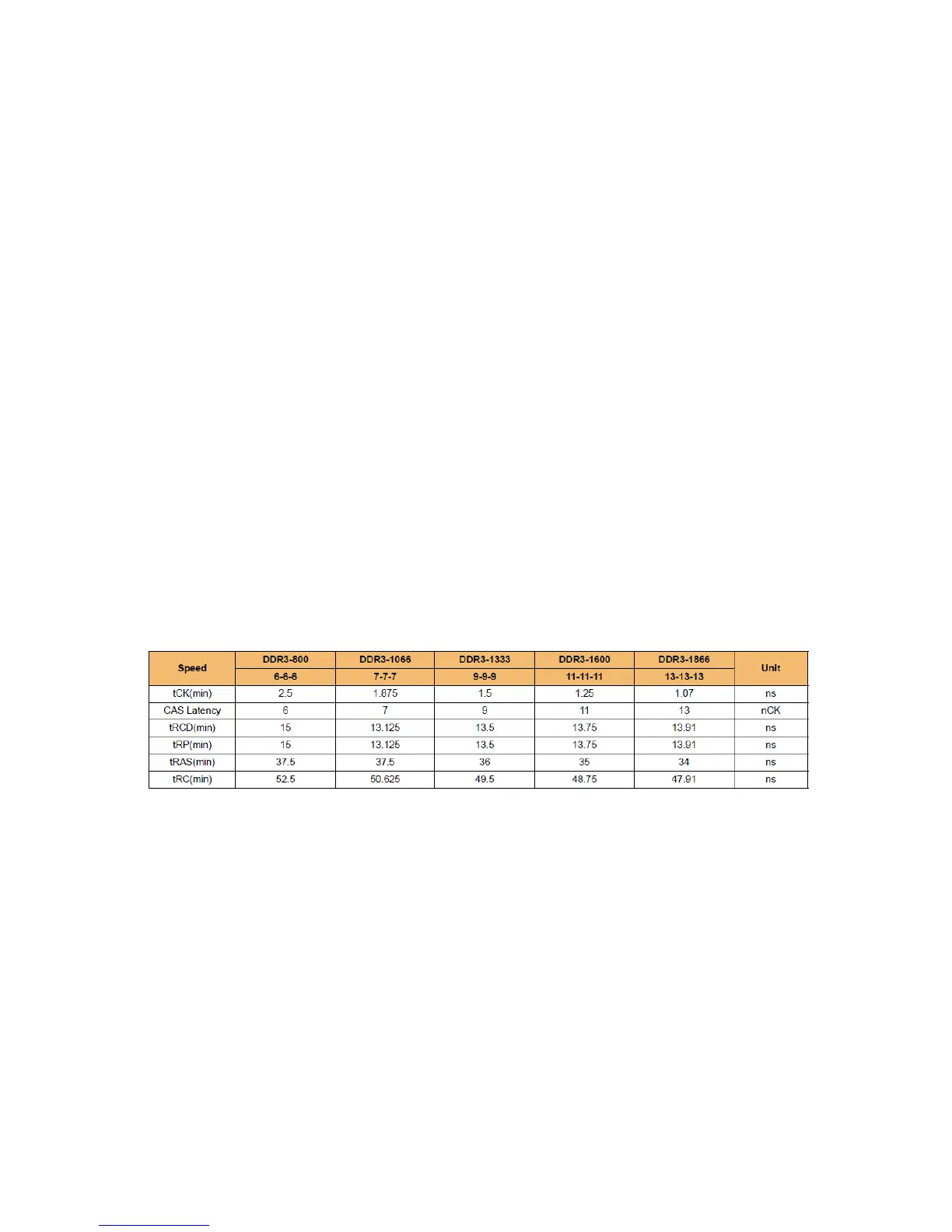
Table 12: 1Gb DDR3 G-die Speed bins
b) Description
The 1Gb DDR3 SDRAM G-die is organized as a 32Mbit x 4 I/Os x 8banks, 16Mbit x 8
I/Os x 8banks device. This synchronous device achieves high speed double-data-rate transfer
rates of up to 1866Mb/sec/pin (DDR3- 1866) for general applications.
The chip is designed to comply with the following key DDR3 SDRAM fea-tures such as
posted CAS, Programmable CWL, Internal (Self) Calibration, On Die Termination using
ODT pin and Asynchronous Reset.
All of the control and address inputs are synchronized with a pair of exter-nally supplied
differential clocks. Inputs are latched at the crosspoint of dif-ferential clocks (CK rising and