30
CK falling). All I/Os are synchronized with a pair of bidirectional strobes (DQS and DQS) in
a source synchronous fash-ion. The address bus is used to convey row, column, and bank
address information in a RAS/CAS multiplexing style. The DDR3 device operates with a
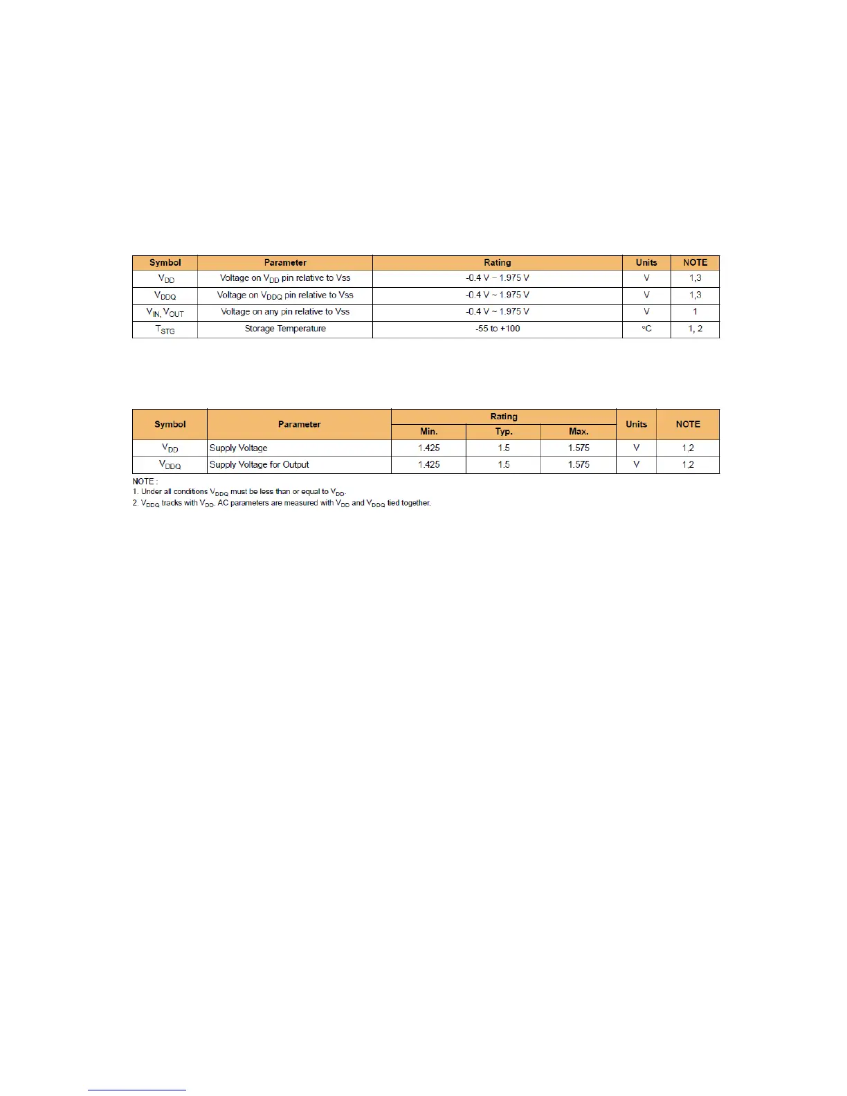
single 1.5V ± 0.075V power supply and 1.5V ± 0.075V VDDQ. The 1Gb DDR3 G-die device
is available in 78ball FBGAs(x4/x8).
Table 13: Absolute Maximum DC Ratings
Table 14: Recommended operating conditions
8. 2Gbit (256M x 8 bit) NAND Flash Memory
H27U2G8F2CTR-BC
a) Key Features
DENSITY
- 2Gbit: 2048blocks
Nand FLASH INTERFACE
- NAND Interface
- ADDRESS / DATA Multiplexing
SUPPLY VOLTAGE
- Vcc = 3.0/1.8V Volt core supply voltage for Program,
Erase and Read operations.
MEMORY CELL ARRAY
- X8: (2K + 64) bytes x 64 pages x 2048 blocks
- X16: (1k+32) words x 64 pages x 2048 blocks
PAGE SIZE
- X8: (2048 + 64 spare) bytes