CONFIDENTIAL
2 Schematic Checklist
2.5 RF
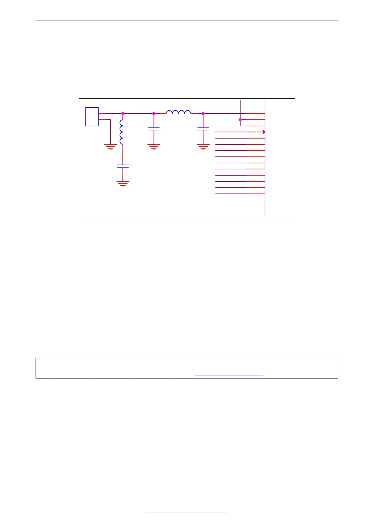
A π-type matching network is essential for antenna matching in the circuit design. CLC structure is
recommended for the matching network. It is also recommended to add an LC filter circuit at the π-type
matching network side to suppress secondary harmonics. The parameters of the components in the matching
network are subject to the actual antenna and PCB layout. Figure 9 shows the RF matching schematic.
5
5
4
4
3
3
2
2
1
1
D D
C C
B B
A A
The values of C11, L2 and C12
vary with the actual PCB board.
The values of C1 and C4 vary with
the selection of the crystal.
The value of R4 varies with the actual
PCB board.
NC: No component.
(Optional)
SPICLK
SPICS0
SPIHD
SPID
SPIWP
SPIQ
SPICS0
LNA_IN
GPIO39
GPIO41
GPIO42
U0RXD
GPIO46
GPIO45
U0TXD
SPICLK
GPIO48
SPID
SPIQ
SPIWP
SPIHD
GPIO9
GPIO8
GPIO7
GPIO6
GPIO5
GPIO4
GPIO3
GPIO2
GPIO1
GPIO0
CHIP_PU
GPIO38
GPIO37
GPIO36
GPIO35
GPIO47
GPIO40
GPIO33
GPIO34
GPIO10
GPIO11
GPIO12
GPIO12
GPIO14
GPIO15
GPIO16
GPIO17
GPIO18
GPIO19
GPIO20
GPIO21
SPICS1 GPIO26
SPICS1
SPICLK
SPIHD
SPID
SPIWP
SPIQ
RF_ANT
VDD_SPI
GND GND GND
VDD33
GND GND GND
GND
VDD33
GND
GND
VDD33
GND
VDD33
GND
GND
GND
VDD_SPI
GND
GND
VDD33
GND
GND
VDD_SPI
GND
GND
GND
GND
C11
TBD
R16 0
C12
TBD
C13
0.1uF
C4
TBD
C15
0.1uF
R3 499
R13 0
C14
1uF
C5
TBD
U1 ESP32-S3
VDDA
56
LNA_IN
1
VDD3P3
2
VDD3P3
3
GPIO0
5
GPIO1
6
GPIO2
7
GPIO3
8
GPIO4
9
GPIO5
10
GPIO6
11
GPIO7
12
GPIO10
15
GPIO11
16
GPIO12
17
GPIO13
18
GPIO14
19
XTAL_32K_P
21
VDD3P3_RTC
20
XTAL_32K_N
22
GPIO17
23
GPIO18
24
GPIO19
25
GPIO20
26
VDD_SPI
29
SPIWP
31
SPICS0
32
SPIQ
34
SPID
35
SPICLK
33
SPICLK_N
36
GND
57
SPICLK_P
37
GPIO33
38
GPIO38
43
GPIO46
52
XTAL_N
53
XTAL_P
54
MTMS
48
MTDO
45
U0TXD
49
VDD3P3_CPU
46
CHIP_PU
4
VDDA
55
MTDI
47
GPIO8
13
GPIO9
14
GPIO21
27
SPICS1
28
SPIHD
30
GPIO34
39
GPIO35
40
GPIO36
41
U0RXD
50
GPIO45
51
GPIO37
42
MTCK
44
C9
TBD
C3
1uF
R15 0
C6
10uF
L1 0
L3
TBD
R1
10K(NC)
U2 FLASH-3V3
VDD
8
GND
4
/CS
1
CLK
6
/HOLD
7
/WP
3
DO
2
DI
5
C10
0.1uF
Y1
40MHz(±10ppm)
XIN
1
GND
2
XOUT
3
GND
4
R4 0
L2 TBD
C7
1uF
U3 PSRAM-3V3
VDD
8
VSS
4
CS
1
SCLK
6
SIO3
7
SIO2
3
SO/SIO1
2
SI/SIO0
5
C1
TBD
ANT1
PCB_ANT
1
2
R10 0
C2
10nF
R14 0
C8
0.1uF
Figure 9: Schematic for RF Matching
2.6 UART
You need to connect a 499 Ω series resistor to the U0TXD line in order to suppress the 80 MHz harmonics.
2.7 ADC
It is recommended to add a 0.1 µF filter capacitor to a pad when using the ADC function. ADC1 is
recommended for use.
2.8 Strapping Pins
Note:
The content below is excerpted from Section Strapping Pins in ESP32-S3 Series Datasheet.
ESP32-S3 has four strapping pins:
• GPIO0
• GPIO45
• GPIO46
• GPIO3
Software can read the values of corresponding bits from register “GPIO_STRAPPING”.
Espressif Systems 13
Submit Documentation Feedback
ESP32-S3 Series Hardware Design Guidelines v1.0
 Loading...