CONFIDENTIAL
2 Schematic Checklist
The rest of this document details the specifics of circuit design for each of these sections.
2.1 Power Supply
Details of using power supply pins can be found in Section Power Scheme in ESP32-S3 Series Datasheet.
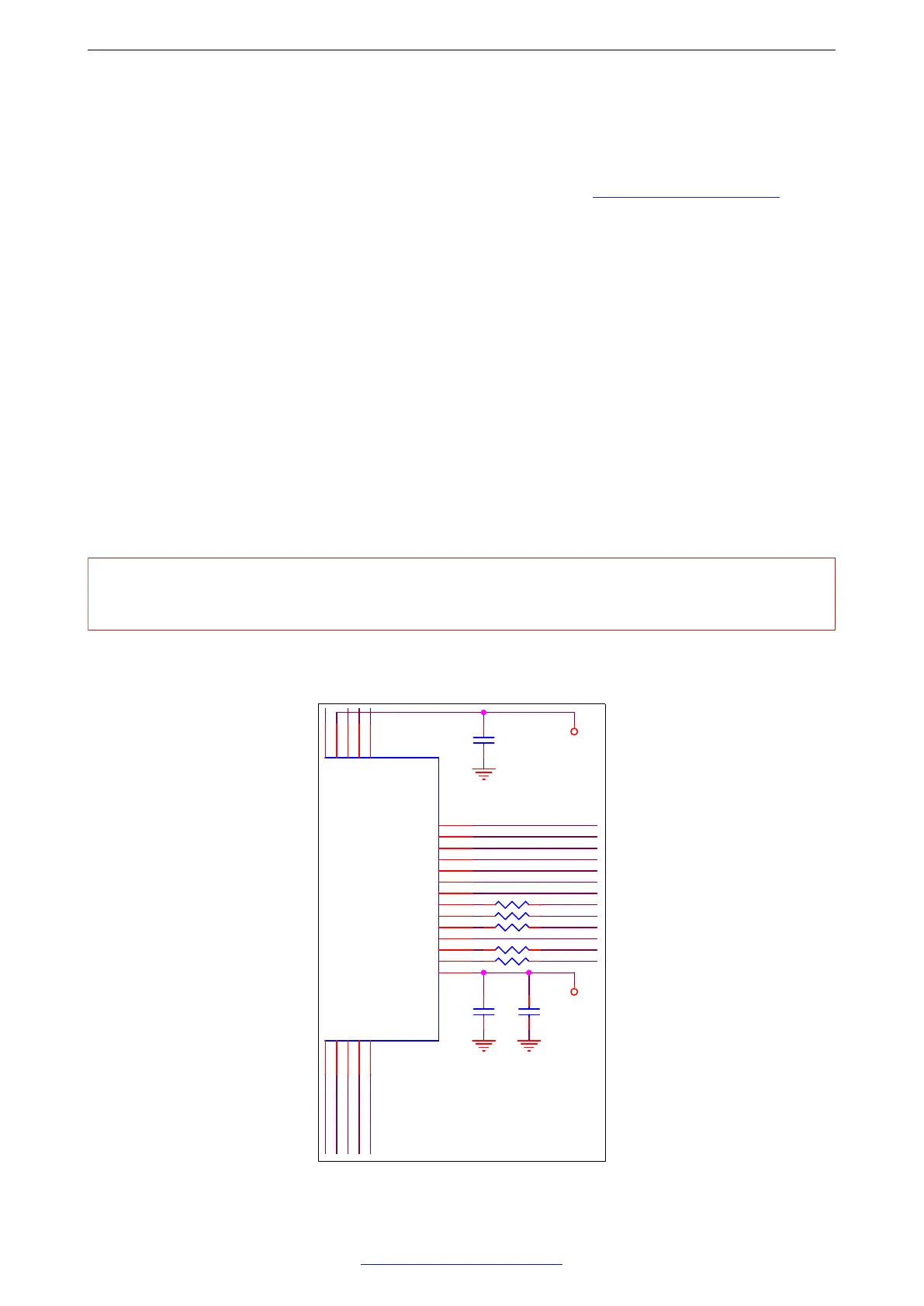
2.1.1 Digital Power Supply
ESP32-S3 has pin46 VDD3P3_CPU that supplies power to CPU IO, in a voltage range of 3.0 V ~ 3.6 V. It is
recommended to add an extra 0.1 µF decoupling capacitor close to each digital power supply pin.
Pin29 VDD_SPI can serve as the power supply for the external device at either 1.8 V if GPIO45 is pulled high
during boot, or at 3.3 V if GPIO45 is pulled low during boot. It is recommended to add extra 0.1 µF and 1 µF
decoupling capacitors close to VDD_SPI.
• When VDD_SPI operates at 1.8 V, it is powered by the internal Flash Voltage Regulator on the chip. The
maximum current this Flash Voltage Regulator can offer is 40 mA.
• When VDD_SPI operates at 3.3 V, it is driven directly by VDD3P3_RTC through R
SP I
resistor, therefore,
there will be some voltage drop from VDD3P3_RTC.
VDD_SPI can also be driven by an external power supply.
Notice:
When using VDD_SPI as the power supply pin for the external 3.3 V flash/PSRAM, the supply voltage should be 3.0 V or
above, so as to meet the requirements of flash/PSRAM’s working voltage.
The schematic for the digital power supply pins is shown in Figure 2.
5
5
4
4
3
3
2
2
1
1
D D
C C
B B
A A
The values of C11, L2 and C12
vary with the actual PCB board.
The values of C1 and C4 vary with
the selection of the crystal.
The value of R4 varies with the actual
PCB board.
NC: No component.
(Optional)
SPICLK
SPICS0
SPIHD
SPID
SPIWP
SPIQ
SPICS0
LNA_INRF_ANT
GPIO39
GPIO41
GPIO42
U0RXD
GPIO46
GPIO45
U0TXD
SPICLK
GPIO48
SPID
SPIQ
SPIWP
SPIHD
GPIO9
GPIO8
GPIO7
GPIO6
GPIO5
GPIO4
GPIO3
GPIO2
GPIO1
GPIO0
CHIP_PU
GPIO38
GPIO37
GPIO36
GPIO35
GPIO47
GPIO40
GPIO33
GPIO34
GPIO10
GPIO11
GPIO12
GPIO12
GPIO14
GPIO15
GPIO16
GPIO17
GPIO18
GPIO19
GPIO20
GPIO21
SPICS1 GPIO26
SPICS1
SPICLK
SPIHD
SPID
SPIWP
SPIQ
VDD_SPI
GND GND GND
VDD33
GND GND GND
GNDGND
VDD33
GND
GND
VDD33
GND
VDD33
GND
GND
GND
VDD_SPI
GND
GND
VDD33
GND
GND
GND
GND
VDD_SPI
R16 0
C11
TBD
C13
0.1uF
C12
TBD
C4
TBD
R3 499
C15
0.1uF
C14
1uF
R13 0
C3
1uF
C9
0.1uF
U1 ESP32-S3
VDDA
56
LNA_IN
1
VDD3P3
2
VDD3P3
3
GPIO0
5
GPIO1
6
GPIO2
7
GPIO3
8
GPIO4
9
GPIO5
10
GPIO6
11
GPIO7
12
GPIO10
15
GPIO11
16
GPIO12
17
GPIO13
18
GPIO14
19
XTAL_32K_P
21
VDD3P3_RTC
20
XTAL_32K_N
22
GPIO17
23
GPIO18
24
GPIO19
25
GPIO20
26
VDD_SPI
29
SPIWP
31
SPICS0
32
SPIQ
34
SPID
35
SPICLK
33
SPICLK_N
36
GND
57
SPICLK_P
37
GPIO33
38
GPIO38
43
GPIO46
52
XTAL_N
54
XTAL_P
53
MTMS
48
MTDO
45
U0TXD
49
VDD3P3_CPU
46
CHIP_PU
4
VDDA
55
MTDI
47
GPIO8
13
GPIO9
14
GPIO21
27
SPICS1
28
SPIHD
30
GPIO34
39
GPIO35
40
GPIO36
41
U0RXD
50
GPIO45
51
GPIO37
42
MTCK
44
L1 2.0nH
C6
10uF
R15 0
Y1
40MHz(±10ppm)
XIN
1
GND
2
XOUT
3
GND
4
C10
0.1uF
U2 FLASH-3V3
VDD
8
GND
4
/CS
1
CLK
6
/HOLD
7
/WP
3
DO
2
DI
5
R1
10K(NC)
U3 PSRAM-3V3
VDD
8
VSS
4
CS
1
SCLK
6
SIO3
7
SIO2
3
SO/SIO1
2
SI/SIO0
5
C7
1uF
L2 TBD
ANT1
PCB_ANT
1
2
C1
TBD
R10 0
R4 0
C2
10nF
C8
0.1uF
R14 0
Figure 2: Schematic for the Digital Power Supply Pins
Espressif Systems 7
Submit Documentation Feedback
ESP32-S3 Series Hardware Design Guidelines v1.0
 Loading...