CONFIDENTIAL
3 PCB Layout Design
3 PCB Layout Design
This chapter introduces the key points of how to design an ESP32-S3 PCB layout using the
ESP32-S3-WROOM-1 module as an example.
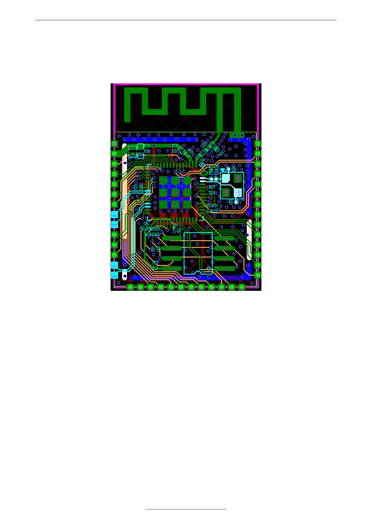
Figure 11: ESP32S3 PCB Layout
3.1 General Principles of PCB Layout
It is recommended to use a four-layer PCB design:
• Layer 1 (TOP): Signal traces and components
• Layer 2 (GND): No signal traces here to ensure a complete GND plane
• Layer 3 (POWER): GND plane should be applied to better isolate the RF and crystal oscillator parts. It is
acceptable to route signal traces on this layer, provided that there is a complete GND plane under the RF
and crystal oscillator.
• Layer 4 (BOTTOM): Route power traces here. It is not recommended to place any components on this layer.
A two-layer PCB design can also be used:
• Layer 1 (TOP): Signal traces and components
• Layer 2 (BOTTOM): Do not place any components on this layer and keep traces to a minimum. Ideally, it
should be a complete GND plane.
Espressif Systems 17
Submit Documentation Feedback
ESP32-S3 Series Hardware Design Guidelines v1.0
 Loading...