BitsyXb - User Manual
36 110118-0001A
I
2
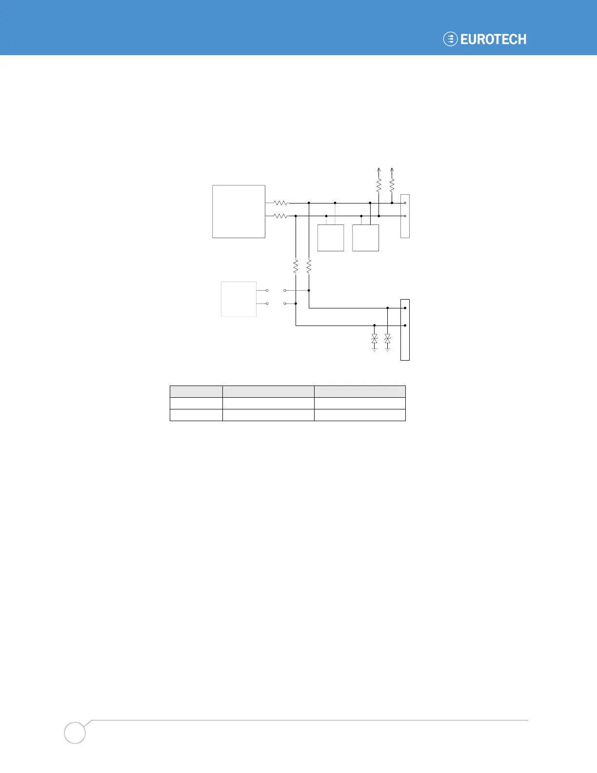
C on the BitsyXb
The BitsyXb uses the processor as the I
2
C bus controller to communicate with the real-time clock
(section 4.2) and the CPU core voltage controller. I
2
C can also be used to communicate with
external devices.
The following diagram illustrates the I
2
C architecture on BitsyXb.
J10
Voltage
Control
RTC
Vddx
SCL
SDA
R117
R26
R3
R194
.49
.11
I2C_SCL
I2C_SDA
R128
R28
Z31
ADSmartIO
PC7
PC6
XScale
R135
R27
J7
.1
.2
Z11
SCL
SDA
The following table lists the addresses of the I
2
C devices on the Bitsy Xb.
The DS1307 supports a maximum bit rate of 100 kbps. Do not use the I
2
C bus at rates faster than
100 kbps.
The BitsyXb I
2
C signals are available on connectors J7 and J10. Electrical specifications are listed
in section 6.3.9.
The ADSmartIO can emulate an I
2
C bus master using PC6 as SCL and PC7 as SDA and can be
connected to the I
2
C bus for backward compatibility with older Bitsy family products. Standard
BitsyXb systems do not connect the ADSmartIO controller to the I
2
C bus.