Feature Reference
110118-0001A 37
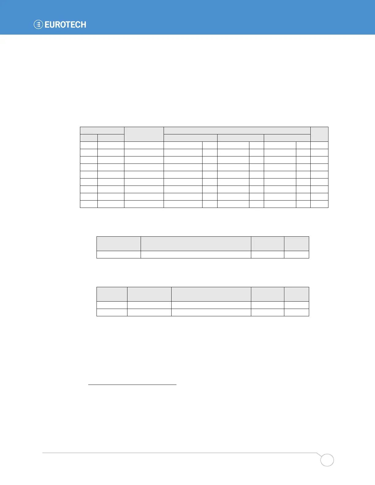
4.5.5 Secure Digital (SD/SDIO) and Multimedia Card (MMC) Controller
The BitsyXb supports Secure Digital Memory (SD), Secure Digital I/O (SDIO), MultiMedia Card
(MMC) and synchronous serial (SPI) modes of operation. SD and SDIO cards can run in 4-bit, 1-
bit and SPI modes. MMC cards run in 1-bit or SPI modes. The PXA270 SD/MMC controller has
FIFOs that support Direct Memory Access (DMA) to and from memory.
Signals for the MMC controller are brought out to header J7. This manual lists the signals for use
in 4-bit SDIO mode. The following table illustrates how the signals are mapped differently
depending on the mode of operation. Signal names and types denote the direction of the signal
relative to the BitsyXb.
14
name
pin
/MMC_CS1
/MMC_CS0
15
The BitsyXb provides a signal to control power to the Secure Digital socket. An external circuit,
usually just a power transistor and related pull-ups, is required to make use of this signal.
BitsyX name Description Type
Power Enable (driven by CPLD)
Some Secure Digital sockets supply the following signals, which are not part of the SD/SDIO
standard. These signals are also connected on header J7.
SD pin BitsyX name Description Type
Operating system drivers may not be available for all modes of operation. Contact Eurotech for
driver availability for the operating system you are using.
Eurotech provides an adapter (170115-020R) that brings these signals out to a Secure Digital
socket. It includes power control circuitry and required pull-up resistors. The adapter can plug
onto a bare BitsyXb (no personality board) or cable out to a location off the BitsyXb. Schematics
and additional details are available on the Eurotech support site.
14
The Secure Digital standard references SPI-mode signals with respect to the card. Pin 2 of the
SD header is listed as "Data In". This user manual and PXA270 documents reference the signals
with respect to the socket. Pin 2 is listed as "Data Out".
15
In SPI mode, pin 9 of an SD/MMC card is unused. Chip Select 0 is shown in this row to
illustrate the alternate signal mapping to SD_DAT2 and would normally be routed to pin 1 of an
SD/MMC socket. Chip Select 0 is not used on the BitsyXb.