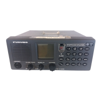
5.4 Block Description
5-7
CH70 receiving signal(156.525 MHz) inputted from the antenna reduce out-of-band
signals/noise with BPF (L/C) of 20 MHz and uses Q3 (RF AMP) to amplify it by
approximately 10 dB. Then, FL2 (SAW FIL, BW:
10 kHz) is installed in order to
improve “Blocking” efficiency. CR6 and 7 are 1
st
MIXER circuit that converts 156.525
MHz into 1
st
local of 118.1625 MHz and 1
st
IF signal of 38.3625 MHz.
156.525 MHz - 118.1625 MHz = 38.3625 MHz
118.1625 MHz is created by multiplying TCXO output of 23.6325 MHz (
2.5 ppm)
with Q8. 1
st
IF signal, after being amplified by Q2 and Q4, and then is converted into
2
nd
IF signal of 37.5 kHz by 2
nd
MIXER circuit of CR4/5 and 2
nd
local signal of 38.4
MHz received from CPU board.
38.3625 MHz - 38.4 MHz = 37.5 kHz
This 37.5kHz signal is inputted into CPU board as CH70 IF OUT signal and is
demodulated with CODEC and DSP.
CH70 IF out:
-measures no modulation signal input with J3 - #5 on CH70 RX board.
CH70 SP SINAD:
-measures SP output (1W) of 1 kHz/70 % MOD.
Fig. 5.4.2 Input/Output characteristic on CH70 RX board
--10 0 10 20 30 40 50 60 70 80 90 100
110dBuV
-60
-50
-40
-30
-20
SSG Level
Level(dBm)SINAD(dB)
-10
0
10
20dB
0.77Vrms
2.15Vrms
7.7mVrms
CH70 IF out
CH70 SP SINAD
1mVrms

 Loading...