2.2 Microcontroller with DSP Module
The hardware is designed around 32 bit controller housed in small 100 pin SMD package. It is a high
speed fix point controller having MIPS’s M4K® 32-bit core with 5-stage pipeline capable of operating
up to 80 MHz.This controller is referred to as MCU (Microcontroller unit).
2.2.1 Microcontroller Module (processor board) Features
• 512K Flash memory (plus an additional 12 KB of Boot Flash)
• 128K on chip SRAM memory
• Multiple interrupt vectors with individually programmable priority
• Fail-Safe Clock Monitor mode
• Configurable Watchdog Timer with on-chip Low-Power RC oscillator for reliable operation
• Internal 8 MHz and 32 kHz oscillators
• Six UART modules with:
• RS-232, RS-485, USB and LIN support
• Four SPI modules
• Five I2C™ modules
• Hardware Real-Time Clock and Calendar (RTCC)
• Five 16-bit Timers/Counters
2.3 Microcontroller and Analog Measurement
P253 hardware supports 4 analog inputs. The relay hardware uses an external 16 bit ADC converter
with capability to sample 8 signals simultaneously to avoid any phase angle error and achieve higher
accuracy. In P253, only 4 channels of ADC converter are used. This external ADC can measure input
in a range of – 10 V to +10 V. The ADC interface uses a SPI serial interface to avoid any software
delays. The MCU continuously monitors different analog signals like line and E/F currents through
CTs, multiplexer and ADC.
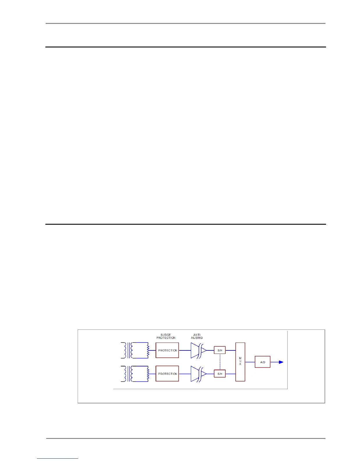
The relay is designed for 5 amp and 1 amp CT secondary current signal. These inputs are further
scaled down to low voltage signal by using an internal current and transformer. The internal current
transformer converts nominal current signal to 3.3 mA. These analog signals are then passed through
protection circuit, anti aliasing filter and amplifier which scales analogue signal to required ADC range.
This anti aliasing filter blocks all high frequency components and surges to avoid measurement error.
The sample and hold (S/H) circuit and multiplexer sample all analog signals at same instant to avoid
and phase angle error and give maximum accuracy.
 Loading...