Troubleshooting
3–9
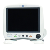
3.3 Display board components
S1
S2
H1
H2
X2
D3
1
82 42
41
Figure 3-3. Display board—front
X1
1
2
29
30
TP4
TP2
TP3
TP1
TP5
TP6
TP15
TP18
TP8
TP9
TP13
TP12
TP16
TP17
TP14
TP10
TP11
Figure 3-4. Display board—back
D3 LCD
H1 LED, external power, green
H2 LED, alarm, bicolor, red/yellow
S1 Power button switch
S2 Alarm Silence button switch
X1 Connector, board-to-board, 30 pin
X2 Backlight
Display board test points
NOTE: TP7 is not used. TP1 through TP6, TP8, and TP9 are for unused pins.
Test point Signal name Description
TP10 V_ON 3 V continuous supply
TP11 V_ON 3 V continuous supply
TP12 ALARM_LED_RED Red alarm LED
TP13 ALARM_LED_YEL IR alarm LED
TP14 FB Feedback for TPS77001 regulator (1.22 V)
TP15 BATT+ Battery + terminal
TP16
__________
LCD_EN
Enables the 4.2 V regulator for display drivers
TP17 CLK Display driver chip; external clock input for display driver
TP18
______
sync
Display driver chip; cascade synchronization IN/OUT
 Loading...