B-44 L60 Line Phase Comparison System GE Multilin
B.4 MEMORY MAPPING APPENDIX B
B
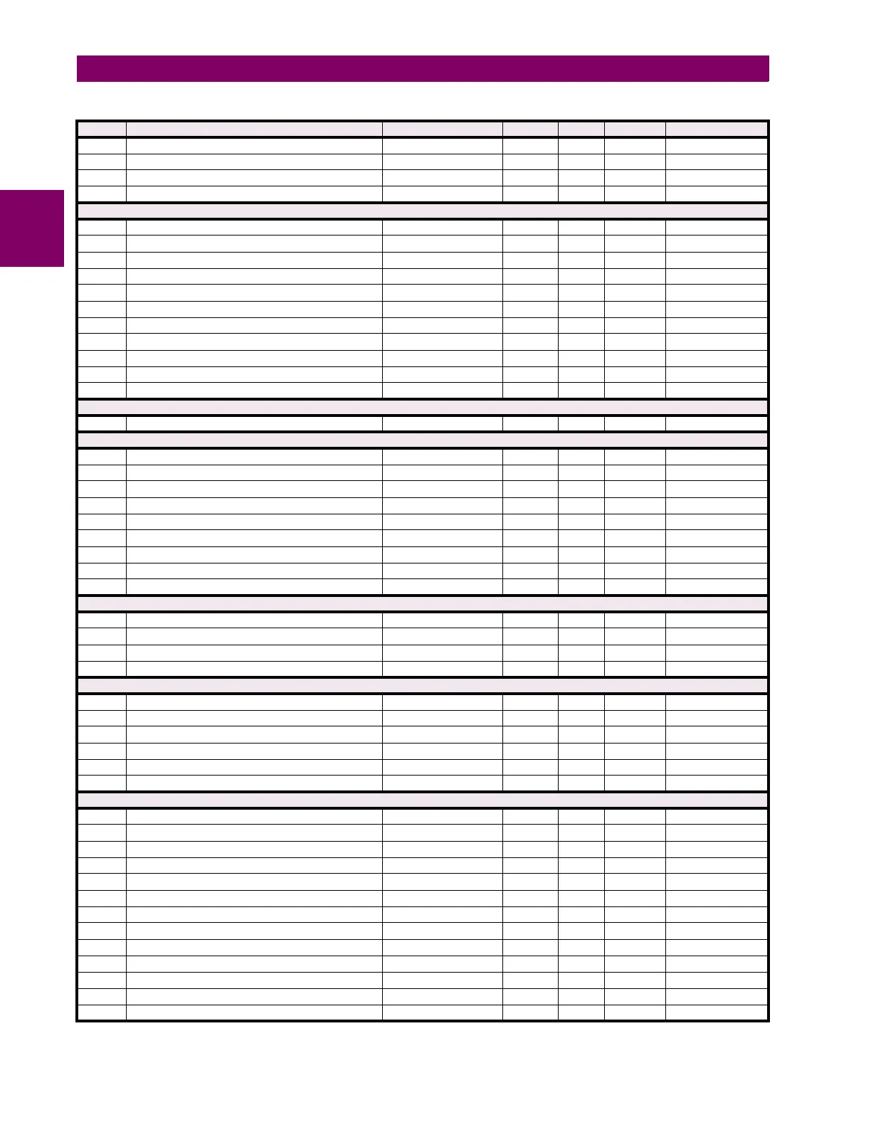
9A09 FlexElement™ 5 Actual
-2147483.647 to 2147483.647
--- 0.001 F004 0
9A0B FlexElement™ 6 Actual
-2147483.647 to 2147483.647
--- 0.001 F004 0
9A0D FlexElement™ 7 Actual
-2147483.647 to 2147483.647
--- 0.001 F004 0
9A0F FlexElement™ 8 Actual
-2147483.647 to 2147483.647
--- 0.001 F004 0
Teleprotection Inputs/Outputs (Read/Write Settings)
9B00 Teleprotection Function 0 to 1 --- 1 F102 0 (Disabled)
9B01 Teleprotection Number of Terminals 2 to 3 --- 1 F001 2
9B02 Teleprotection Number of Channels 1 to 2 --- 1 F001 1
9B03 Teleprotection Local Relay ID 0 to 255 --- 1 F001 0
9B04 Teleprotection Terminal 1 ID 0 to 255 --- 1 F001 0
9B05 Teleprotection Terminal 2 ID 0 to 255 --- 1 F001 0
9B06 Reserved (10 items) 0 to 1 --- --- F001 0
9B10 Teleprotection Input 1-n Default States (16 items) 0 to 3 --- 1 F086 0 (Off)
9B30 Teleprotection Input 2-n Default States (16 items) 0 to 3 --- 1 F086 0 (Off)
9B50 Teleprotection Output 1-n Operand (16 items) 0 to 65535 --- 1 F300 0
9B70 Teleprotection Output 2-n Operand (16 items) 0 to 65535 --- 1 F300 0
Teleprotection Inputs/Outputs Commands (Read/Write Command)
9B90 Teleprotection Clear Lost Packets 0 to 1 --- 1 F126 0 (No)
Teleprotection Channel Tests (Read Only)
9B91 Teleprotection Channel 1 Status 0 to 2 --- 1 F134 1 (OK)
9B92 Teleprotection Channel 1 Number of Lost Packets 0 to 65535 --- 1 F001 0
9B93 Teleprotection Channel 2 Status 0 to 2 --- 1 F134 1 (OK)
9B94 Teleprotection Channel 2 Number of Lost Packets 0 to 65535 --- 1 F001 0
9B95 Teleprotection Network Status 0 to 2 --- 1 F134 2 (n/a)
9BA0 Teleprotection Channel 1 Input States 0 to 1 --- 1 F500 0
9BA1 Teleprotection Channel 2 Input States 0 to 1 --- 1 F500 0
9BB0 Teleprotection Input 1 States, 1 per register (16 items) 0 to 1 --- 1 F108 0 (Off)
9BC0 Teleprotection Input 2 States, 1 per register (16 items) 0 to 1 --- 1 F108 0 (Off)
Charge current compensation settings (read/write
9EF0 Charging current compensation factor 0 to 1 --- 1 F102 0 (Disabled)
9EF1 Charging current compensation block 0 to 65535 --- 1 F300 0
9EF2 Charging current compensation positive-sequence Xc 0.100 to 65.535 kohms 0.001 F001 100
9EF3 Charging current compensation zero-sequence Xc 0.100 to 65.535 kohms 0.001 F001 100
VT Fuse Failure (Read/Write Setting) (6 modules)
A040 VT Fuse Failure Function 0 to 1 --- 1 F102 0 (Disabled)
A041 ...Repeated for module number 2
A042 ...Repeated for module number 3
A043 ...Repeated for module number 4
A044 ...Repeated for module number 5
A045 ...Repeated for module number 6
Permissive overreach transfer trip (POTT) settings (read/write)
A070 POTT Scheme Function 0 to 1 --- 1 F102 0 (Disabled)
A071 POTT Permissive Echo 0 to 1 --- 1 F102 0 (Disabled)
A072 POTT Rx Pickup Delay 0 to 65.535 s 0.001 F001 0
A073 POTT Transient Block Pickup Delay 0 to 65.535 s 0.001 F001 20
A074 POTT Transient Block Reset Delay 0 to 65.535 s 0.001 F001 90
A075 POTT Echo Duration 0 to 65.535 s 0.001 F001 100
A076 POTT Line End Open Pickup Delay 0 to 65.535 s 0.001 F001 50
A077 POTT Seal In Delay 0 to 65.535 s 0.001 F001 400
A078 POTT Ground Direction OC Forward 0 to 65535 --- 1 F300 0
A079 POTT Rx 0 to 65535 --- 1 F300 0
A07A POTT Echo Lockout 0 to 65.535 s 0.001 F001 250
A07B POTT Target 0 to 2 --- 1 F109 0 (Self-reset)
A07C POTT Events 0 to 1 --- 1 F102 0 (Disabled)
Table B–9: MODBUS MEMORY MAP (Sheet 36 of 55)
ADDR REGISTER NAME RANGE UNITS STEP FORMAT DEFAULT

 Loading...