PRODUCT OVERVIEW S3C84BB/F84BB
PIN DESCRIPTIONS (IC74)
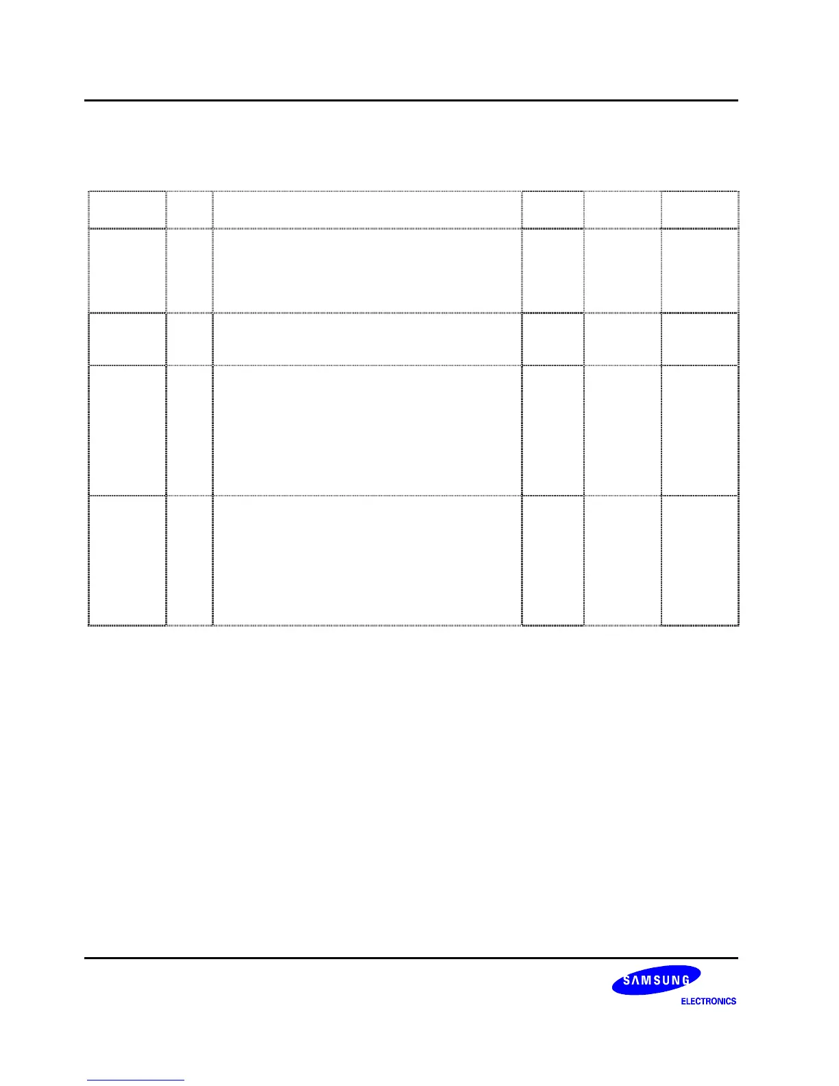
Table 1-1. S3C84BB/F84BB Pin Descriptions (80-QFP)
Pin
Name
Pin
Type
Pin
Description
Circuit
Type
Pin
Number
Share
Pins
P0.0 - P0.7 I/O Bit programmable port; input or output mode
selected by software; input or push-pull output.
Software assignable pull-up.
Alternately, P0.0-P0.7 can be used as the PG
output port (PG0-PG7).
D 80-73 PG0-PG7
P1.0 - P1.7 I/O Bit programmable port; input or output mode
selected by software; input or push-pull output.
Software assignable pull-up.
D 72-65
P2.0 - P2.7 I/O Bit programmable port; input or output mode
selected by software; input or push-pull output.
Software assignable pull-up.
Alternately, P2.0~P2.7 can be used as I/O for
TIMERA, TIMERB, D/A, SIO
D,D-2 8-1 SO
SI
SCK
DAOUT
TBPWM
TACK
TACAP
TAOUT
P3.0 - P3.7 I/O Bit programmable port; input or output mode
selected by software; input or push-pull output.
Software assignable pull-up.
Alternately, P3.0~P3.7 can be used as I/O for
TIMERC0/C1, TIMER10/11
D 30–23 T1CK0
T1CK1
T1CAP0
T1CAP1
T1OUT0
T1OUT1
TCOUT0
TCOUT1
 Loading...