14
OPERATION
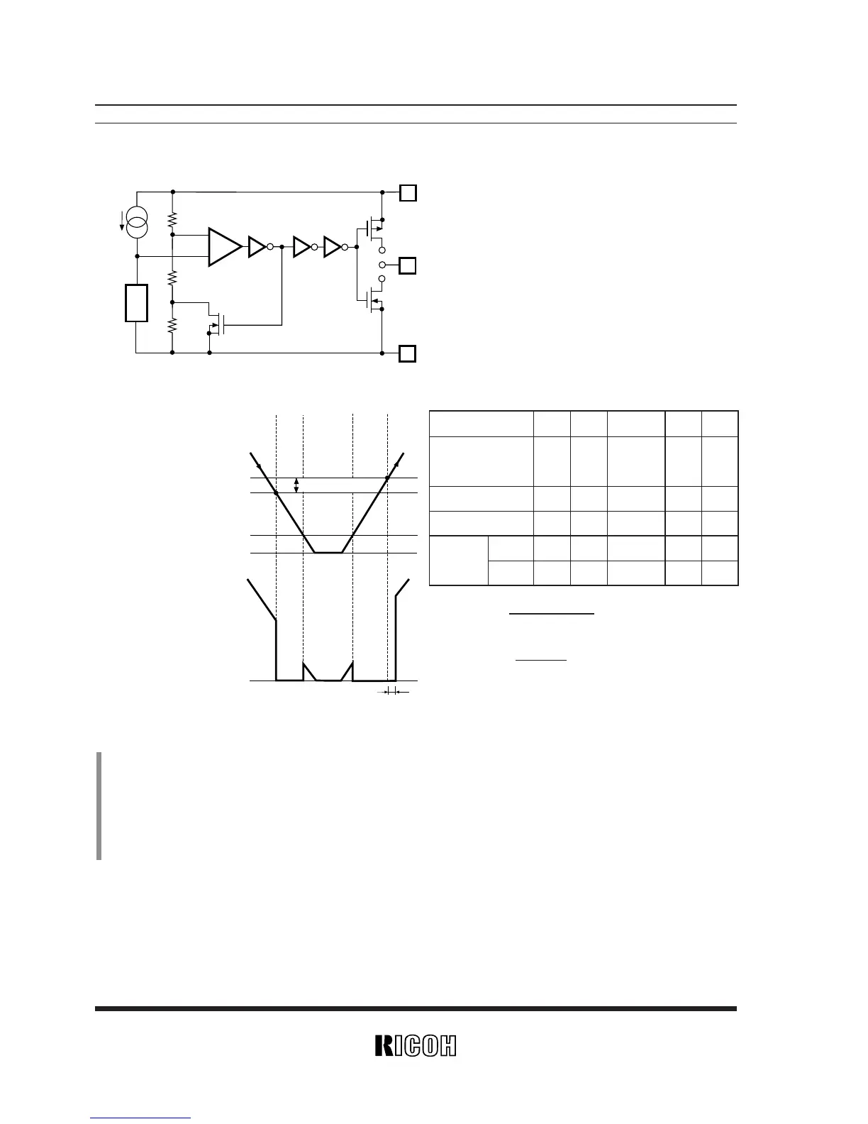
FIG. 1 Block Diagram
Operation Diagram
Step 1. Output Voltage is equal to Power Source Voltage (VDD).
Step 2. When Input Voltage to Comparator reaches the state of Vref≥V
DD
·(Rb+Rc)/(Ra+Rb+Rc)at Point A (Detected Voltage –VDET), the output of Com-
parator is reserved, so that Output Voltage becomes GND.
Step 3. In the case of CMOS Output, Output Voltage becomes unstable when Supply Voltage (V
DD) is smaller than Minimum Operating Voltage. In the
case of Nch Open Drain Output, a pulled-up voltage is output.
Step 4. Output Voltage becomes equal to GND.
Step 5. When Input Voltage to Comparator reaches the state of Vref≤V
DD· (Rb)/(Ra+ Rb) at Point B (Released Voltage +VDET), the output of Comparator is reversed,
so that Output Voltage becomes equal to Supply Voltage (V
DD).
FIG. 2 Operation Diagram
Step Step 1 Step 2 Step 3 Step 4 Step 5
Comparator(+) Pin
Input Voltage
I II II II I
Comparator Output
H L
Indefinite
L H
Tr. 1 OFF ON
Indefinite
ON OFF
Output Tr.
Pch ON OFF
Indefinite
OFF ON
Nch OFF ON
Indefinite
ON OFF
I
.
Rb + Rc
Ra + Rb + Rc
·V
DD
II
.
Rb
Ra + Rb
·V
DD
• In R×5VT××A, Nch Tr. drain is
connected to OUT pin.
• In R
×5VT××C, Nch Tr. drain
and Pch Tr. drain are connected
to OUT pin.
Released Volage +V
DET
Supply Volage Detected Volage –V
DET
(V
DD
)
Minimum Operating Volage
GND
Output Volage
(OUT)
GND

 Loading...