PRODUCT OVERVIEW S3C84BB/F84BB
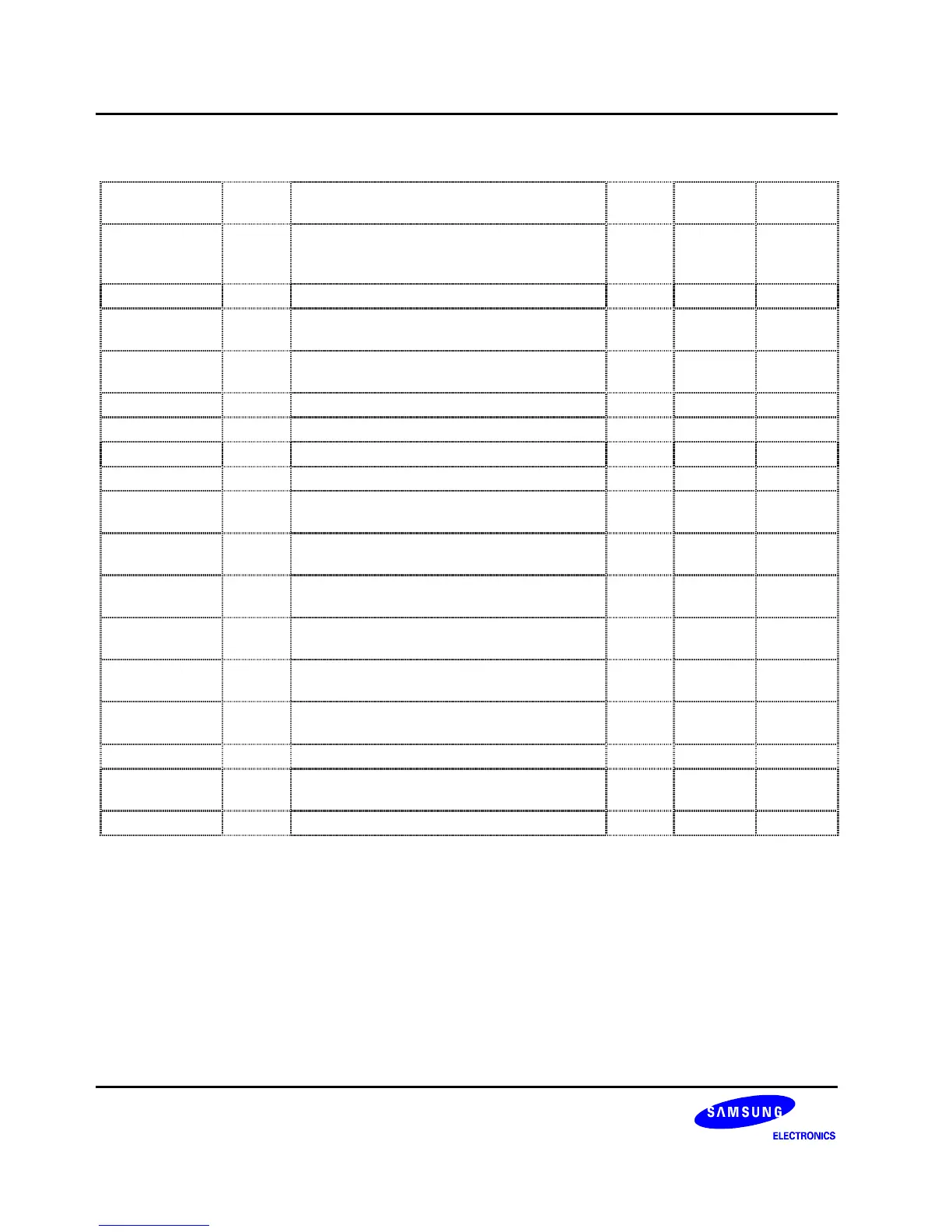
Table 1-1. S3C84BB/F84BB Pin Descriptions (80-QFP) (Continued)
Pin
Name
Pin
Type
Pin
Description
Circuit
Type
Pin
Number
Share
Pins
AD0 - AD7 I Analog input pins for A/D converter module.
Alternatively used as general-purpose digital
input port 7.
E 48–45
42–39
P7.0–P7.7
AVREF, AVSS - A/D converter reference voltage and ground - 43, 44 -
RxD0, RxD1 I/O Serial data RxD pin for receive input and
transmit output (mode 0)
D 18, 21 P5.3, P5.1
TxD0, TxD1 O Serial data TxD pin for transmit output and
shift clock input (mode 0)
D 20, 22 P5.2, P5.0
TACK I External clock input pins for timer A D 3 P2.5
TACAP I Capture input pins for timer A D 2 P2.6
TAOUT O Pulse width modulation output pins for timer A D 1 P2.7
TBPWM O Carrier frequency output pins for timer B D 4 P2.4
TCOUT0
TCOUT1
O Timer C 8-bit PWM mode output or counter
match toggle output pins
D 24,23 P3.6,P3.7
T1CK0
T1CK1
I External clock input pins for timer 1 D 39,30 P3.0,P3.1
T1CAP0
T1CAP1
I Capture input pins for timer 1 D 28,27 P3.2,P3.3
T1OUT0
T1OUT1
O Timer 1 16-bit PWM mode output or counter
match toggle output pins
D 26,25 P3.4,P3.5
SI,SO,SCK I/O Synchronous SIO pins D 7,8,9 P2.1,P2.0,
P2.2
RESETB I
System reset pin (pull-up resistor: 240 kΩ)
B 19 -
TEST I Pull – down register connected internally - 16 -
VDD1, VDD2,
VSS1, VSS2
- Power input pins - 12,53,
13,52
-
XIN, XOUT - Main oscillator pins - 15,14 -
 Loading...