Handling of Unused Pin
The unused I/O pins should be processed appropriately as below.
Classification Pin Name Setting
Analog RX0-7, LOUT1-4, ROUT1-4, LIN, RIN These pins should be open.
INT0-1, BOUT, XTO, MCKO1-2, COUT, UOUT,
VOUT, SDTO1-2, CDTO, DZF1-2, TX1-0
These pins should be open.
CSN, DAUX1-2, SDTI1-4, XTL0-1
These pins should be connected to DVSS.
Digital
TEST1-3 These pins should be connected to PVSS.
ASAHI KASEI [AK4589]
No. Pin Name I/O Function
55 AVDD - Analog Power Supply Pin, 4.75V∼5.25V
56 AVSS -
Analog Ground Pin, 0V
57 RX0 I Receiver Channel 0 Pin (Internal biased pin. Internally biased at PVDD/2)
58 NC -
No Connect pin
No internal bonding. This pin should be connected to PVSS.
59 RX1 I Receiver Channel 1 Pin (Internal biased pin. Internally biased at PVDD/2)
60 TEST1 I
Test 1 Pin
This pin should be connected to PVSS.
61 RX2 I Receiver Channel 2 Pin (Internal biased pin. Internally biased at PVDD/2)
62 NC -
No Connect pin
No internal bonding. This pin should be connected to PVSS.
63 RX3 I Receiver Channel 3 Pin (Internal biased pin. Internally biased at PVDD/2)
64 PVSS - PLL Ground pin
65 R -
External Resistor Pin
12k
Ω
+/-1% resistor should be connected to PVSS externally.
66 PVDD -
PLL Power supply Pin, 4.75V∼5.25V
67 RX4 I Receiver Channel 4 Pin (Internal biased pin. Internally biased at PVDD/2)
68 TEST2 I
Test 2 Pin
This pin should be connected to PVSS.
69 RX5 I Receiver Channel 5 Pin (Internal biased pin. Internally biased at PVDD/2)
70 CAD0 I
Chip Address 0 Pin (ADC/DAC part)
71 RX6 I Receiver Channel 6 Pin (Internal biased pin. Internally biased at PVDD/2)
72 CAD1 I
Chip Address 1 Pin (ADC/DAC part)
73 RX7 I Receiver Channel 7 Pin (Internal biased pin. Internally biased at PVDD/2)
74 I2C I
Control Mode Select Pin.
“L”: 4-wire Serial, “H”: I
2
C Bus
75 DAUX2 I Auxiliary Audio Data Input Pin (DIR/DIT part)
76 VIN I V-bit Input Pin for Transmitter Output
77 MCLK I
Master Clock Input Pin
78 TX0 O Transmit Channel (Through Data) Output 0 Pin
79 TX1 O
Transmit Channel Output1 pin
When DIT bit = “0”, Through Data.
When DIT bit = “1”, DAUX2 Data.
80 INT0 O Interrupt 0 Pin
Note: All input pins except internal biased pins and Analog input pins (RX0-7, LIN, RIN) should not be left floating.
VCOM
PVDD
PVSS
RX pin
20k(typ)
20k(typ)
Internal biased pin Circuit
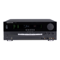
AVR340 harman/kardon
 Loading...