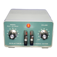
Page 35
r-
~=*---*$+:--3
CIRCUIT DESCRIPTION
Refer to the Schematic (fold-out from Page 43)
when the Keyer is on. The fuse provides pro-
and Block Diagram while reading the Circuit
tection in case of a short circuit.
Description.
The output of power transformer T1
is
recti-
fied by silicon diode D2
and
filtered by ca-
SCHEMATIC DIAGRAM
The letter -number designations on the Schematic
Diagram are used to identify resistors, capac-
itors, and diodes. Each designation is related
by
the first number to the transistor stage in
which it is used. For example, the resistors
in
transistor stage Q1 are designated R10, R11,
etc. In transistor stage Q7 they are designated
R70, R71, etc.
Letter-number designations using numbers 1
through
9
are not directly related to any tran-
sistor stage. This system of circuit component
designations
is
used throughout the Schematic.
Circled letter designations on the Schematic
Diagram indicate wire connecting locations on
the circuit board.
pacitor C2 to produce a positive
(+)
19-volts
DC. Silicon diode D3 and a filter network con-
sisting of capacitors C3 and C4 and resistor
R9
provides a negative
(-)
16 volts DC. These
voltages are the operating and bias voltages
for the transistor stages.
KEY SWITCHING
The key lever is moved in one direction or the
other to actuate switch S1 or S2. Switch S1
turns on the dot generator multivibrator circuit
to produce dots. Switch S2 turns on the flip-flop
and the dot generator multivibrators to produce
dashes. The operation of these circuits will be
explained later.
DOTS
POWER SUPPLY Dot Clamp Circuit
With slide switch S3 in the Operate or Hold When the key lever
is
in the center (neutral)
position, the AC line voltage
is
applied across position, a positive voltage
is
present at the base
the primary winding of power transformer TI.
of
dot clamp transistor Q3. This voltage which
Resistor R8 drops the line voltage that
is
ap-
is
applied from the power supply through re-
plied to the neon pilot lamp, which indicates sistors R1, R5, and R6, biases
Q3
in an on
I
I
DOT DASH
CLAMP
-
.
CLAMP
Q
3
Q
6
SPEED
AND
DOT-SPACE
RATIO
-
KEY
LEVER
+I9
-16
VDC VDC
POWER
SUPPLY
I
I
tr'
120
VAC
OUTPUT
-)TO
TRANSMITTER
DOT
GENERATOR
-0-MULTIVIBRATOR
Q1
Q2
A UD
I0
CLAMP
FLIP-FLOP DELAY
DRIVER
SWITCH
MULTIVIBRATOR
+
FOLLOWER
lRCUl
c
(14
05
-
(37
o
e
.
L
BLOCK DIAGRAM