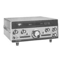
Page
320
TRANSMITTER
Refer to the 'Transmitter Block Diagram," fold-out from
Page
268.
The Transmitter AudiolRegulator circuit board accepts the
microphone, key, and phone patch inputs, which
it
processes and controls.
It
regulates the
5
and
11
volt DC
voltages used throughout the Transceiver. The functions
located on this circuit board are the audio preamplifiers, the
VOX and PTT circuits, the keying circuits, the CW
sidetone
generator, the relay driver, the SSBICW control, and the
aforementioned voltage regulators.
The Carrier
GeneratorICrystal Filter circuit board contains
the balanced modulator, which mixes the transmitter audio
and the appropriate carrier
(BFO). The carrier is then
balanced out, leaving a double sideband signal, one sideband
of which
is
removed by the crystal filter,
The
3395
kHz
IF signal
is
amplified on the Transmitter
IFIPredriver circuit board. The IF signal and the premix
signal are combined in the balanced mixer, and are then
passed through a
bandpass filter, after which they are again
amplified. Keying
is
accomplished at this point by turning
these amplifiers on and off. The amplifiers are followed by a
second group of
bandpass filters, which are followed by the
Driver circuit board.
The HFO signals for the various bands are generated by
crystal oscillators on the
HFOIPremix circuit board. These
signals are mixed with the VFO output to form a premix
signal, which is then filtered by a group of
bandpass filters.
5000
-
jrjo0KH-t
The VFO operates over a range of
500
kHz.
Its
output
is
fed
to the
HFOIPremix board, where
it
is
processed as
a
component of the premix signal. The VFO output level
is
increased on the
28.0
-
29.5
MHz bands by the VFOIfilter
switch.
The Driver circuit amplifies the signal to the level required
to drive the Power Amplifier. However, the Driver output
can also
be
switched to bypass the Power Amplifier and
furnish a
QRP signal direct to the FilterIALC board and the
antenna. Part of the output
is
rectified and used for ALC
voltage in the low power mode.
The Power Amplifier consists essentially of two push-pull
amplifiers operated in parallel. Their bias voltage
is
furnished
by a diode mounted in the heat sink, so the bias voltage
tracks with the heat sink temperature to prevent thermal
runaway. The circuit
is
broad-banded and no tuning of the
power amplifier output circuit
is
required.
The
FilterlALC circuit board contains low-pass filters to
attenuate harmonics which must be suppressed to prevent
interference to other services. Solid-state switching
is
used to
change the ALC time constant for
SSB and CW. Part of the
power output
is
rectified and connected to the panel meter
for the Relative Power indication.
DISPLAY
Refer to the Display Block Diagram on Page
271.
f
The frequency display is processed on two circuit boards
-
the counter board and the display board.
On the counter board, a stable crystal oscillator acts as the
time base, calibrated against station
WWV. A divider string
and associated gates provide the gate, transfer, and reset
pulses.
If the BFO frequency is subtracted from the premix
frequency, the result
is
the signal frequency. Therefore, the
counter
is
automatically preset to start counting below an
arbitrary
0
by the amount of the BFO frequency. In this
way, the entire premix frequency
is
counted but only the
signal frequency
is
displayed.
When the transfer pulse occurs, the count is transferred from
five counters to memory latches, which retain the count at
their outputs for the duration of the counting cycle.
The Display circuit board contains segment drivers, five of
which receive and process the count from the memory
latches. The drivers turn on the appropriate elements in the
display tubes.
The first (left-hand) digit of the display iscontrolled by the
band switch
so
the digit will be unlighted or show a
"1"
or a
"2"
as appropriate for the Band switch position.