HLK-LD2420
user manual
3.hardware description
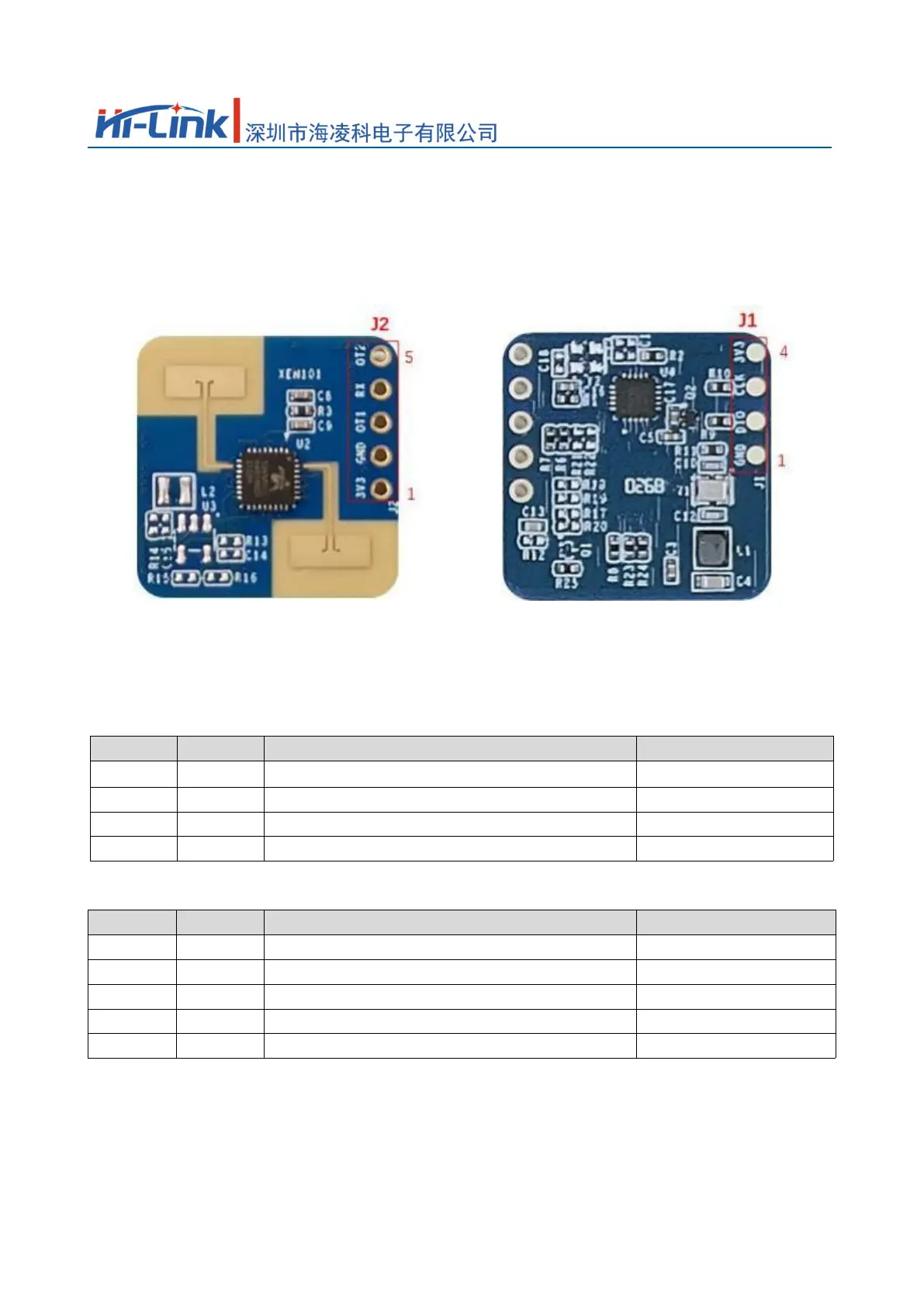
The picture below shows the front and back photos of the module. Module reserved5A pin hole (the factory does not match the pin) is calledJ2, for power supply and communication;J1for
SWDinterface forMCUProgram burning and debugging.
front reverse side
picture3-1The physical picture of the front and back of the module
surface3-1 J1Pin Description
J#PIN# name Function illustrate
J1Pin1 GND grounding -
J1Pin2 DIO SWD interface data cable 0 ~ 3.3V
J1Pin3 CLK SWD interface clock line 0 ~ 3.3V
J1Pin4 3V3 power input 3.0V ~ 3.6V, Typ.3.3V
surface3-2 J2Pin Description
J#PIN# name Function illustrate
J2Pin1 3V3 power input 3.0 V ~ 3.6 V, Typ.3.3 V
J2Pin2 GND grounding -
J2Pin3 OT1 UART_TX 0 ~ 3.3V
J2Pin4 RX UART_RX 0 ~ 3.3V
J2Pin5 OT2 IO, used to report the detection status: high level means there are people, low level means no one 0 ~ 3.3V
illustrate:J1,J2Interface pin spacing2.54 mm.
HLK-LD2420supportKeil 5 IDEburninghexfile or source code project, you can useJ-Link (V9above version),
CMSIS-DAPWait for the programmer to download the program. Please make sure it is installed before burningPuya.PY32F0xx_DFP.1.1.0.pack.
4total pages15Page
 Loading...