K6602705
Rev.3
08.20.01
- 105 -
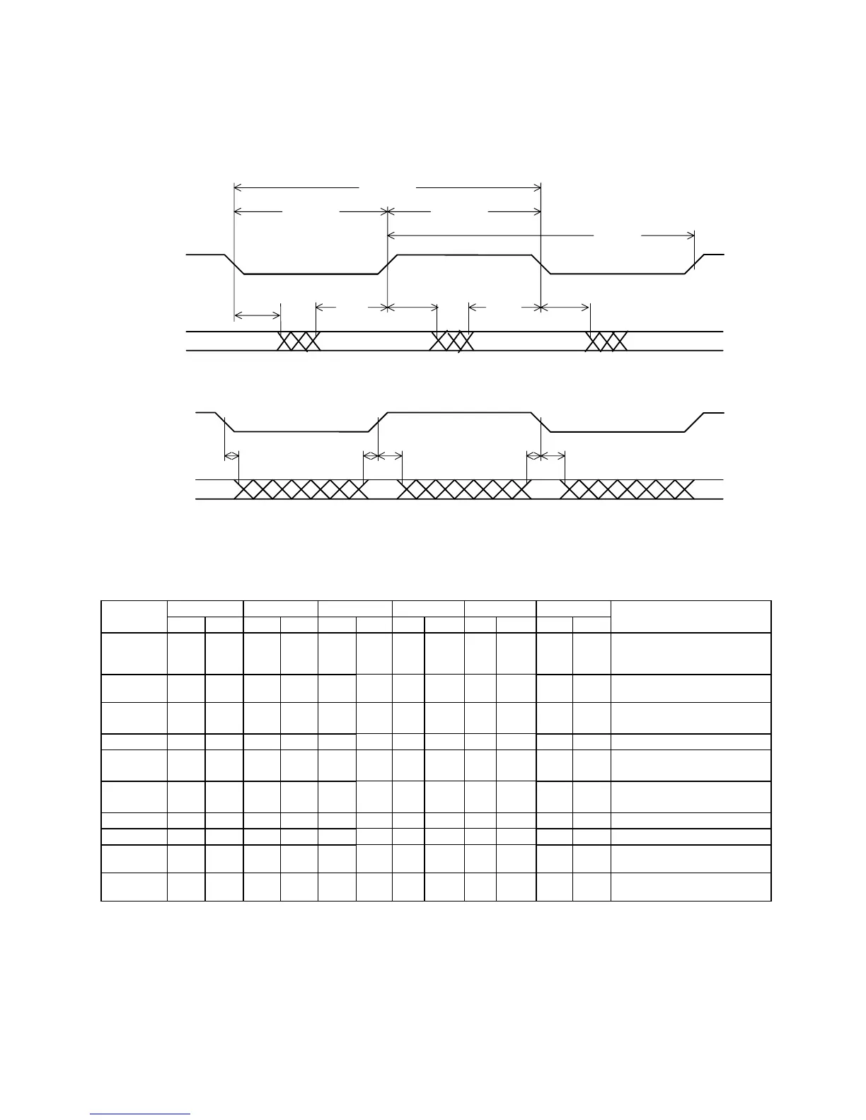
Figure 6-14 Sustained Ultra DMA Write Data
t
DH
t
DS
t
DVH
HSTROBE
at host
DD(15:0)
at host
HSTROBE
at device
DD(15:0)
at device
t
DVH
t
CYC
t
CYC
t
DVS
t
DVS
t
DS
t
DH
t
2CYC
t
DH
t
DVH
t
2CYC
t
DVHIC
t
DVSIC
t
DVHIC
t
DVSIC
t
DVHIC
t
DHIC
t
DSIC
t
DHIC
t
DSIC
t
DHIC
Note: DD(15:0) and HSTROBE signals are shown at both the device and the host to emphasize that cable settling
time as well as cable propagation delay shall not allow the data signals to be considered stable at the device until
some time after they are driven by the host.
Mode 0(ns) Mode 1(ns) Mode 2(ns) Mode 3(ns) Mode 4(ns) Mode5(ns) Description
SYMBOL MIN MAX MIN MAX MIN MAX MIN MAX MIN MAX MIN MAX
t
CYC
112 73 54 39 25 16.8
Cycle time allowing for
asymmetry and clock
variation
t2
CYC
230 153 115 86 57 38
Two cycle time allowing for
clock variation
t
DS
15 10 7 7 5 4 Data setup time at
recipient
t
DH
5 5 5 5 5 4.6 Data hold time at recipient
t
DVS
70 48 31 20 6.7 4.8 Data valid setup time at
sender
t
DVH
6.2 6.2 6.2 6.2 6.2 4.8 Data valid hold time at
sender
t
DSIC
14.7 9.7 6.8 6.8 4.8 2.3
Recipient IC data setup time
t
DHIC
4.8 4.8 4.8 4.8 4.8 2.8
Recipient IC data hold time
t
DVSIC
72.9 50.9 33.9 22.6 9.5 6.0
Sender IC data valid setup
time
t
DVHIC
999996
Sender IC data valid hold
time
 Loading...