Rev. 1.71 102 April 11, 2017 Rev. 1.71 103 April 11, 2017
HT66F002/HT66F0025/HT66F003/HT66F004
Cost-Effective A/D Flash MCU with EEPROM
HT66F002/HT66F0025/HT66F003/HT66F004
Cost-Effective A/D Flash MCU with EEPROM
AlthoughtheA/Dclocksourceisdeterminedbythesystemclockf
SYS
,andbybitsSACK2~SACK0,
therearesomelimitationsonthemaximumA/Dclocksourcespeedthatcanbeselected.Asthe
recommendedvalueofpermissibleA/Dclockperiod,t
ADCK
,isfrom0.5μsto10μs,caremustbe
takenforsystemclockfrequencies.Forexample,ifthesystemclockoperatesatafrequencyof
4MHz,theSACK2~SACK0bitsshouldnotbesetto000Bor11xB.DoingsowillgiveA/Dclock
periodsthatarelessthantheminimumA/DclockperiodorgreaterthanthemaximumA/Dclock
periodwhichmayresultininaccurateA/Dconversionvalues.
Controllingthepoweron/offfunctionoftheA/Dconvertercircuitryisimplementedusingthe
ENADCbitintheSADC0register.ThisbitmustbesethightopowerontheA/Dconverter.When
theENADCbitissethightopowerontheA/Dconverterinternalcircuitryacertaindelay,as
indicatedinthetimingdiagram,mustbeallowedbeforeanA/Dconversionisinitiated.Evenifno
pinsareselectedforuseasA/Dinputsbyconguringthecorrespondingpin-sharedcontrolbits,if
theENADCbitishighthensomepowerwillstillbeconsumed.Inpowerconsciousapplicationsit
isthereforerecommendedthattheENADCissetlowtoreducepowerconsumptionwhentheA/D
converterfunctionisnotbeingused.
ThereferencevoltagesupplytotheA/DConvertercanbesuppliedfromeithertheinternalADCpower
orfromanexternalreferencesourcessuppliedonpinVREForV
BG
voltage.Thedesiredselectionis
madeusingtheSAVRS3~SAVRS0bits.AstheVREFpinispin-sharedwithotherfunctions,whenthe
VREFpinisselectedasthereferencevoltagesupplypin,theVREFpin-sharedfunctioncontrolbits
shouldbeproperlyconguredtodisableotherpinfunctions.WhenV
REF
orV
BG
isselectedbyADC
inputorADCreferencevoltage,theOPAneedstobeenabledbysettingENOPA=1.
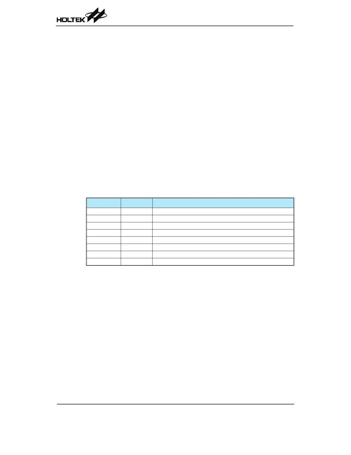
Reference SAVRS[3:0] Description
AV
DD
0000 ADC Reference Voltage comes from AV
DD
V
REF
0001 ADC Reference Voltage comes from External V
REF
V
REF
×2 0010 ADC Reference Voltage comes from External V
REF
×2
V
REF
×3 0011 ADC Reference Voltage comes from External V
REF
×3
V
REF
×4 0100 ADC Reference Voltage comes from External V
REF
×4
V
BG
×2 1010 ADC Reference Voltage comes from V
BG
×2
V
BG
×3 1011 ADC Reference Voltage comes from V
BG
×3
V
BG
×4 1100 ADC Reference Voltage comes from V
BG
×4
A/D Converter Reference Voltage Selection
A/D Converter Input Signal
AlloftheA/Danaloginputpinsarepin-sharedwiththeI/OpinsonPortAandPortBaswellas
otherfunctions.ThecorredpondingselectionbitsforeachI/OpininthePASRandPBSRregisters,
determinewhethertheinputpinsaresetupasA/Dconverteranaloginputsorwhethertheyhave
otherfunctions.Ifthepin-sharedfunctioncontrolbitscongureitscorrespondingpinasanA/D
analogchannelinput,thepinwillbesetuptobeanA/Dconverterexternalchannelinputandthe
originalpinfunctionsdisabled.Inthisway,pinscanbechangedunderprogramcontroltochange
theirfunctionbetweenA/Dinputsandotherfunctions.Allpull-highresistors,whicharesetup
throughregisterprogramming,willbeautomaticallydisconnectedifthepinsaresetupasA/D
inputs.NotethatitisnotnecessarytorstsetuptheA/DpinasaninputinthePACandPBCport
controlregistertoenabletheA/Dinputaswhenthepin-sharedfunctioncontrolbitsenableanA/D
input,thestatusoftheportcontrolregisterwillbeoverridden.
TheA/Dconverterhasitsownreferencevoltagepin,VREF,howeverthereferencevoltagecan
alsobesuppliedfromthepowersupplypin,achoicewhichismadethroughtheSAVRS[3:0]inthe
SADC2register.TheanaloginputvaluesmustnotbeallowedtoexceedthevalueofV
REF.