Rev. 1.71 10 April 11, 2017 Rev. 1.71 11 April 11, 2017
HT66F002/HT66F0025/HT66F003/HT66F004
Cost-Effective A/D Flash MCU with EEPROM
HT66F002/HT66F0025/HT66F003/HT66F004
Cost-Effective A/D Flash MCU with EEPROM
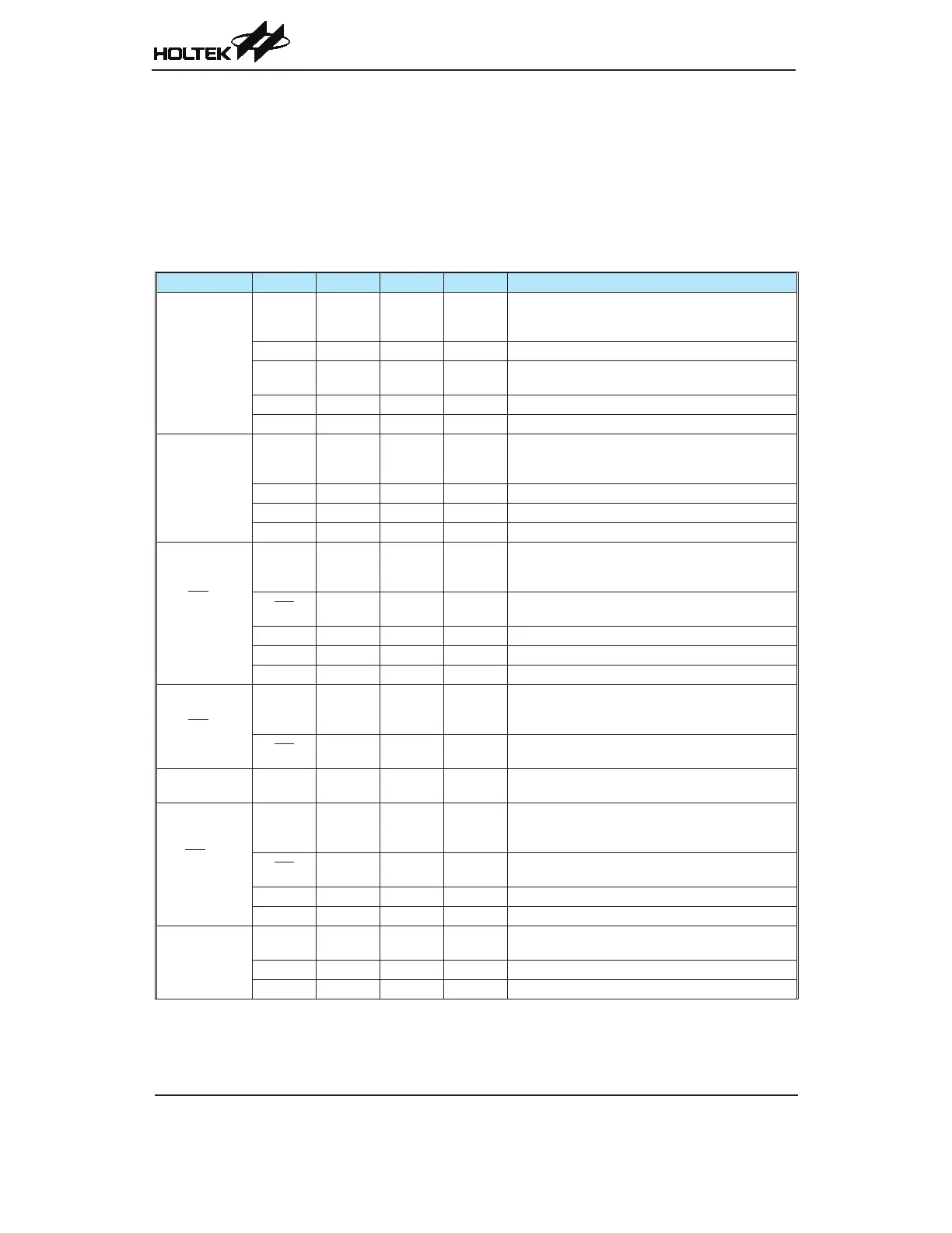
Pin Description
Withtheexceptionofthepowerpinsandsomerelevanttransformercontrolpins,allpinsonthese
devicescanbereferencedbytheirPortname,e.g.PA0,PA1etc,whichrefertothedigitalI/O
functionofthepins.HoweverthesePortpinsarealsosharedwithotherfunctionsuchastheAnalog
toDigitalConverter,TimerModulepinsetc.Thefunctionofeachpinislistedinthefollowingtable,
howeverthedetailsbehindhoweachpiniscongurediscontainedinothersectionsofthedatasheet.
HT66F002/HT66F0025
Pin Name Function OPT I/T O/T Description
PA0/[STP0]/
[STP0I]/AN0/
ICPDA
PA0
PAWU
PAPU
PASR
ST CMOS
General purpose I/O. Register enabled pull-up and
wake-up
STP0 PASR — CMOS TM0 (STM) output
STP0I
PASR
IFS0
ST — TM0 (STM) input
AN0 PASR AN — ADC input channel 0
ICPDA — ST CMOS ICP Data Line
PA1/[STP0B]/
AN1/VREF
PA1
PAWU
PAPU
PASR
ST CMOS
General purpose I/O. Register enabled pull-up and
wake-up
STP0B PASR — CMOS TM0 (STM) inverting output
AN1 PASR AN — ADC input channel 1
VREF PASR AN — ADC VREF Input
PA2/[INT]/
STP0/AN2/
VREFO
PA2
PAWU
PAPU
PASR
ST CMOS
General purpose I/O. Register enabled pull-up and
wake-up
INT
PASR
IFS0
ST — External interrupt input
STP0 PASR — CMOS TM0 (STM) output
AN2 PASR AN — ADC input channel 2
VREFO PASR — AN ADC reference voltage output
PA3/[INT]
PA3
PAWU
PAPU
PASR
ST CMOS
General purpose I/O. Register enabled pull-up and
wake-up
INT
PASR
IFS0
ST — External interrupt input
PA4 PA4
PAWU
PAPU
ST CMOS
General purpose I/O. Register enabled pull-up and
wake-up
PA5/INT/
STP0B/AN3
PA5
PAWU
PAPU
PASR
ST CMOS
General purpose I/O. Register enabled pull-up and
wake-up
INT
PASR
IFS0
ST — External interrupt input
STP0B PASR — CMOS TM0 (STM) inverting output
AN3 PASR AN — ADC input channel 3
PA6/STP0I/
[STCK0]
PA6
PAWU
PAPU
ST CMOS
General purpose I/O. Register enabled pull-up and
wake-up
STP0I IFS0 ST — TM0 (STM) input
STCK0 IFS0 ST — TM0 (STM) clock input