8662A Option HI
1
08662-92019
Page 9 of 20
DESCRIPTION OF OPTION Hll MODIFICATION
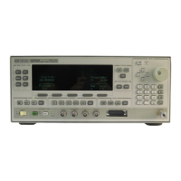
The 8662A with Option HI
1
has been modified so that what formerly was the signal to
enable the AUX FM INPUT, now controls the 10 MHz reference source selected by the A8A4
Reference Buffer board.
This is done by cutting the trace on the A2A10 DCU Motherboard between pin 18 and
pin 3. The AUX FM control signal is then routed to the 10 MHz Reference Oscillator Casting
(A8MP10) through a newly installed 5000pf feedthrough capacitor, onto the A8A5 Reference
Section Motherboard, and then to a special relay circuit on the A8A4 Reference Buffer board.
The AUX FM input circuitry remains intact, but is factory-configured in the "OFF" or
disabled mode as shown on page 19 in the partial figure
8-539
and as described under Section III,
Operation, of this Insert. AUX FM may be wired in the enabled mode on the A4A9 Modulation
Drive board as shown on page 20 in the partial figure
8-539
and as described under Section III,
Operation, of this Insert.
On page 8-402, replace Figure 8-401, A8A4 Reference Buffer Component Locations,
with the new figure on page 14 of this Insert.
On page
8-403
(Service Sheet 18), replace Figure 8-402, A8A3 and A8A4 10 MHz
Reference Oscillator and Buffer Block Diagrams, with the new figure on page 15 of this Insert.
On page
8-403
(Service Sheet 18), add Figure 8-402A, Block Diagram of Option HI
1
Circuitry found on page 16 of this Insert.
On page
8-403
(Service Sheet 18), replace part of Figure 8-403, A8A3 and A8A4 10
MHz Reference Oscillator Buffer Schematic, with the partial schematic on page 17 of this Insert.
On page
8-522
(Service Sheet 40), add Figure 8-537A, A4A9 Auxiliary FM ON-OFF
jumper locations, found on page 18 of this insert.
On page 8-523/8-524 (Service Sheet 40), replace part of Figure 8-539, A4A9 Modulation
Drive Schematic, with the partial schematics on page 19 and 20 of this Insert.
Copyright 1986 - HEWLETT-PACKARD COMPANY - Spokane Division
24001 E. Mission Avenue, Liberty Lake, WA 99019-9599 U.S.A.