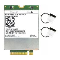
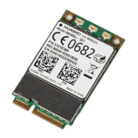
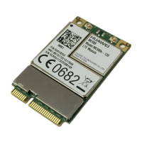
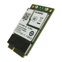
HUAWEI ME909 Series LTE LGA Module
Hardware Guide
Description of the Application Interfaces
Huawei Proprietary and Confidential
Copyright © Huawei Technologies Co., Ltd.
Figure 3-16 Circuit diagram of the interface of the PCM (ME909 is used as PCM master)
PCM_SYNC: Output when PCM is in master mode;
PCM_CLK: Output when PCM is in master mode;
The PCM function of ME909 is only supported in master mode.
It is recommended that a TVS be used on the related interface, to prevent electrostatic
discharge and protect integrated circuit (IC) components.
The signal level of CODEC must match that of the ME909 module.
3.9 General Purpose I/O Interface
The ME909 module provides 5 GPIO pins for customers to use for controlling signals
which are worked at 1.8 V CMOS logic levels. Customers can use AT command to
control the state of logic levels of 5 GPIO output signal. See the HUAWEI
ME909u-521 LTE LGA Module AT Command Interface Specification.
Table 3-11 Signals on the GPIO interface
 Loading...
