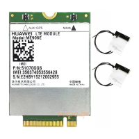
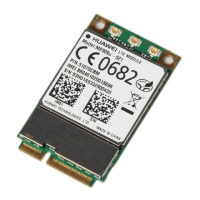
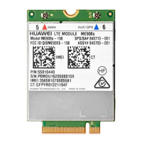
HUAWEI MU609 HSPA LGA Module
Hardware Guide
Huawei Proprietary and Confidential
Copyright © Huawei Technologies Co., Ltd.
8-wire UART (Universal Asynchronous Receiver-Transmitter) x 1
2-wire UART x 1 (this is only used for debugging)
GPIO (General-purpose I/O) x 5
LED (Light-Emitting Diode) x 1
JTAG (Joint Test Action Group) interface
Sleep indicator interface (SLEEP_STATUS)
WWAN MAIN antenna pad x1, WWAN AUX antenna pad x 1, GPS
antenna pad x 1
Management of SMS: read SMS, write SMS, send SMS, delete
SMS and list SMS.
Supports MO and MT: Point-to-point
GPRS: UL 85.6 kbit/s; DL 85.6 kbit/s
EDGE: UL 236.8 kbit/s; DL 236.8 kbit/s
WCDMA PS: UL 384 kbit/s; DL 384 kbit/s
HSPA: UL 5.76 Mbit/s; DL 14.4 Mbit/s
[1]: When the MU609 module works in the range of –40°C to –20°C or +70°C to +85°C , NOT all
its RF performances comply with 3GPP specifications.
2.3 Circuit Block Diagram
Figure 2-1 shows the circuit block diagram of the MU609 module. The major
functional units of the MU609 module contain the following parts:
Power management
Baseband controller
Multi-chip package (MCP) memory
RF Circuit

 Loading...


