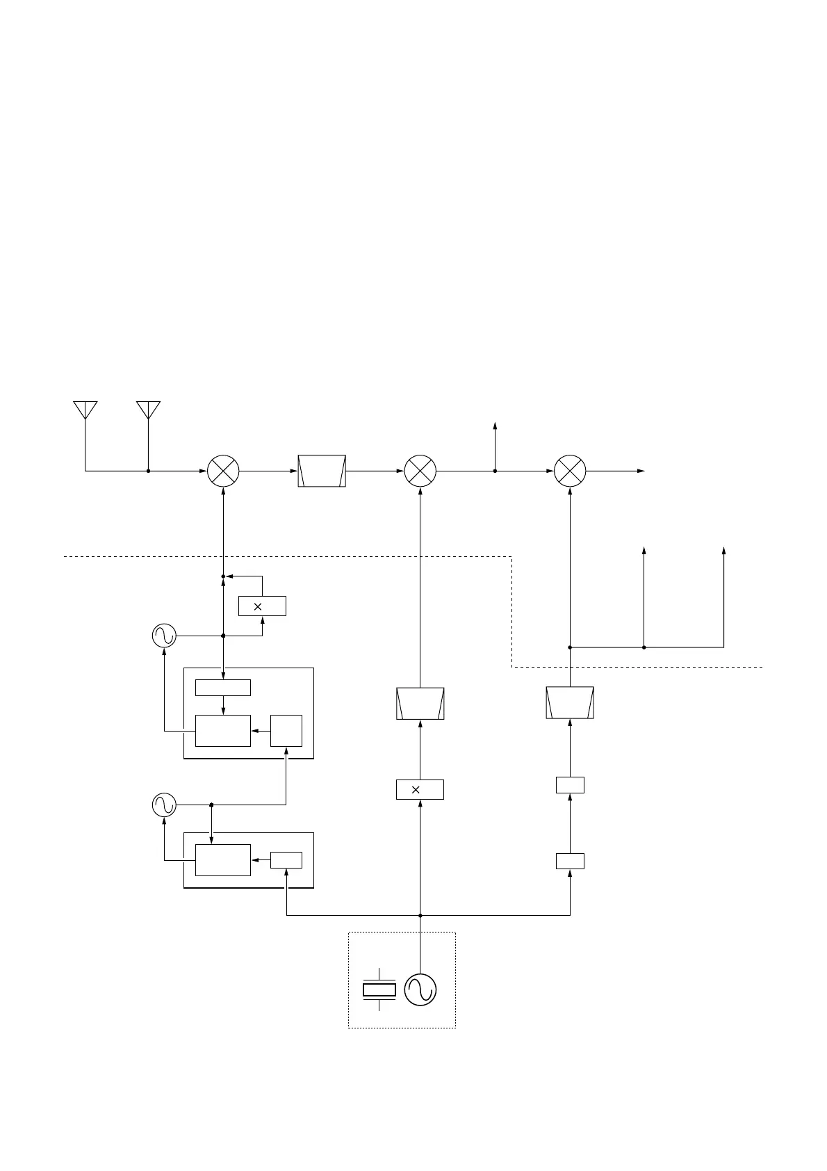
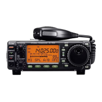
3-3-3 2ND LO AND REFERENCE OSCILLATOR
CIRCUITS
The reference oscillator (X621, Q621) generates a 30.0
MHz frequency used for the 1st LO and BFO circuits as a
system clock and for the 2nd LO signal.
The oscillated signal is amplified at the buffer amplifier
(Q661), and is doubled at Q681 and the 60 MHz frequency
is picked up at the bandpass filter (L681, L682). The 60 MHz
signal is applied to the MAIN board as a 2nd LO signal.
3-3-4 BFO CIRCUIT
The DDS IC (IC901) generates a 10-bit digital signal. The
signal is converted into an analog wave signal at the D/A
converter (R951–R970). The analog wave is passed
through the high-pass filter and low-pass filter. The 9 MHz
BFO signal is then applied to the MAIN board via the “BFO”
signal line.
While transmitting in RTTY mode, the RTTY keying signal is
applied to IC901 pin 3 to shift the generated frequency and
to obtain 2 frequencies for FSK operation.
While receiving in FM or FM narrow mode, the BFO circuit
generates a 9.4665 MHz frequency as the 3rd LO signal.
While transmitting in FM or FM narrow mode, the BFO cir-
cuit generates a 9.0115 MHz or 9.0100 MHz frequency as
the TX FM PLL reference frequency, respectively.