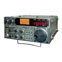
3-1 RECEIVER CIRCUITS
3-1-1 HF/50 MHz RF CIRCUIT
(FILTER, MAIN AND HPF BOARDS)
HF/50 MHz RF filters pass only the desired band signals
and suppress any undesired band signals. The HF/50 MHz
RF circuit has 7 low-pass filters and 8 high-pass filters for
specified band use.
HF/50 MHz RF signals from the [ANT1] connector, pass
through one of 7 low-pass filters as below, the transmit/
receive switching relay (FILTER board; RL1) and low-pass
filter (FILTER board; L1, L2, C1–C5), and are then applied
to the MAIN board via J1 (FILTER board).
The signals from the FILTER board are applied to or bypass
the 20 dB attenuator (R122, R125, R126). The signals pass
through the high-pass filter (L132, L133, C132–C137) to
suppress strong signals below 1.6 MHz and are then applied
to the HPF board via the “SAF” terminal.
(1) 0.03–2 MHz and 30–40 MHz
The signals pass through a low-pass filter (L101, L102,
C101–C105), and then applied to the preamplifier circuit on
the MAIN board.
(2) 2–30 MHz
The signals from the low-pass filter (L101, L102,
C101–C105) are applied to one of 6 high-pass filters as at
right above and are then applied to the preamplifier circuit
on the MAIN board.
(3) 40–60 MHz
The signals pass through the low-pass filter (L172, L173,
C172–C176) and the high-pass filter (L174, L175,
C177–C181) via D171 and are then applied to the preampli-
fier circuit on the MAIN board.
3-1-2 VHF AND UHF RF CIRCUITS (PA UNIT)
The VHF and UHF RF circuits pass and amplify only the
desired band signals and suppresses any undesired band
signals. The both RF circuits have a preamplifier and band-
pass filters respectively.
• VHF RF CIRCUIT
The VHF RF signals from the [ANT2] connector pass
through the low-pass filter (L263–L265, C274–C276) and
antenna switching circuit (D291–D293). The signals are
applied to the bandpass filter (D403, D409, D408), and are
then amplified at the preamplifier circuit (Q403). The ampli-
fied signals are then applied to the another bandpass filter
(D407, D406, D410).
• UHF RF CIRCUIT
The UHF RF signals from the [ANT2] connector pass
through the high-pass filter (L316, L317, C326–C327), low-
pass filter (L313–L315, C322–C324) and antenna switching
circuit (D341, D342, D343). The signals are amplified at the
preamplifier circuit (Q453) between the 2 bandpass filters
(D454, D453 and D454, D456).
The filtered signals are applied to the MAIN board via J481
(PA unit) and are then applied to the preamplifier circuit.
D403, D408, D409, D406, D407, D410, D454, D453, D454
and D456 are varactor diodes that tune the ceinter frequen-
cy of an RF passband for wide bandwidth receiving and
good image response rejection. On the VHF band, receiving
signals are above 129 MHz, the switching diodes (D404,
D405) are turned off by the control signal “2MBL” from PLL
unit, then the varactor diodes (D408, D407) are disconnect-
ed.
• Used RF high-pass filter (HPF board)
• Used RF low-pass filter (FILTER board)