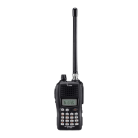
CIRCUIT DESCRIPTION
This charger provides proper charging current for various
battery packs which
is
selected
by
charging current selector
on the bottom of
the
battery pack.
Also a constant charging current
is
provided by controlling
conducting phase angle
of
the
SCR
in
the circuit. It keeps
the current constant even
if
various battery packs which
have different
output
voltage, has been used.
1.
CONDUCTING ANGLE CONTROL CIRCUIT
A gate pulse
is
used
to
control the thyristor (SCR)
in
the
circuit. This gate pulse
is
a part
of
a full-wave rectified
wave and its phase angle
is
controlled by a saw tooth pulse
which
is
synchronized
to
the
full-wave rectified wave.
The pulse
falltime of
the
saw
tooth
pulse
is
controlled by
an actual charging current, and it decides
the
phase angle
of
the gate pulse
of
between
40
degrees and 160 degrees.
The saw tooth pulse generate circuit consists of
02,
05
and
C9.
A full-wave rectified voltage
is
applied
to
the
base
of
02
through
R4
and turns
02
on at near its base line
(D
portion
in
the figure), and charges
C9
to
+9V
which from regulator
01.
When
the
rectified voltage exceeds +9V (out of D
portion),
02
is
turned off and
the
charged voltage
of
C9
is
discharged through
05,
and a saw tooth wave
is
generated
across C9. This saw tooth pulse
is
fed
to
Pin 12 of
IC2.
[\
)I
[\
)
A-3
When
the
pulse voltage decreases
less
than gate's threshold
voltage, Pin
11
of
IC2
puts out H
level
voltage. This turns
04
and
03
on, and a portion of full-wave rectified voltage
is
fed
to
the
gate
of
D6
SCA
through
03,
and
06
is
turned·
on.
When
the
SCA
has been turned on, it holds this condition
until
the
power source voltage becomes zero or its cathode
is
biased
by
reverse voltage. Thus, when
the
full-wave
rectified voltage becomes
less
than
+9V
(D
portion
in
the
figure), the
SCA
will be turned off.
Rated charging current
is
decided
by
R37 - R42. R37 -
R42 are selected by S3 - S5 which are turned on or off by
a battery pack's charging current selector, and are
in
series
with
the
charging battery.
A voltage across R37, R38 or R39 - R42
is
integrated by
R14 and C16, then fed
to
the base
of
06.
05
and
06
compose a differential amplifier. A reference voltage which
is
divided from
+9V
by
R11
and R12,
is
applied
to
the base
of
05,
thus the collector current
of
05
is
varied by the base
voltage of
06,
and controls discharging time
of
C9.
For example, when the charging current increases more
than the specified charging current,
06
collector current
increases,
05
collector current decreases,
C9
discharging
time becomes longer,
the
phase angle
of
D6 gate pulse
delays (the pulse width becomes narrower), and the charg-
ing
current decreases.
When the charging current decreases
less
than
the
specified
charging current,
the
circuit functions the opposite way and
keeps
the
charging current constant.
2. LOGIC CIRCUIT
The logic circuit
is
controlled by
the
charging current select
switches
S3
- S5, and the charging detector
010.
When charging
1C-CM2
or
IC-CM5,
S5
is
turned on by the
charging current selector on the battery pack.
The charging current (600mA) flows through R39 - R42,
and a voltage across these resistors
is
applied
to
the
base
of
010
and turns it on. Thus, a gate input
Pin
1 and 2 of
IC2
becomes L level, its
output
Pin
3 H level. This puts
out
H
level
at Pin 4
of
IC1,
output
of a flip-flop consisting
of
a
gate of ICl and a gate
of
IC2.
Also Pin 10
of
IC1
puts
out
H
level
and
Pin
10 of
IC2
L level.
This grounds
the
emitter
of
04
through R10 and Pin 10 of
IC2,
and
03
is
turned on during
Pin
11
of
IC2
is
H
level
and
charges the battery pack.