FC6A S
ERIES
MICROS
MART
L
ADDER
P
ROGRAMMING
M
ANUAL
FC9Y-B1726 10-21
10: D
ATA
C
ONVERSION
I
NSTRUCTIONS
DTDV (Data Divide)
Valid Devices
For valid device address ranges, see "Device Addresses" on page 2-1.
When T (timer) or C (counter) is used as S1, the timer/counter current value (TC or CC) is displayed.
Destination device D1 uses 2 data registers starting with the device assigned by D1.
Since the DTDV instruction is executed in each scan while input is on, a pulse input from a SOTU or SOTD instruction should be used.
Valid Data Types
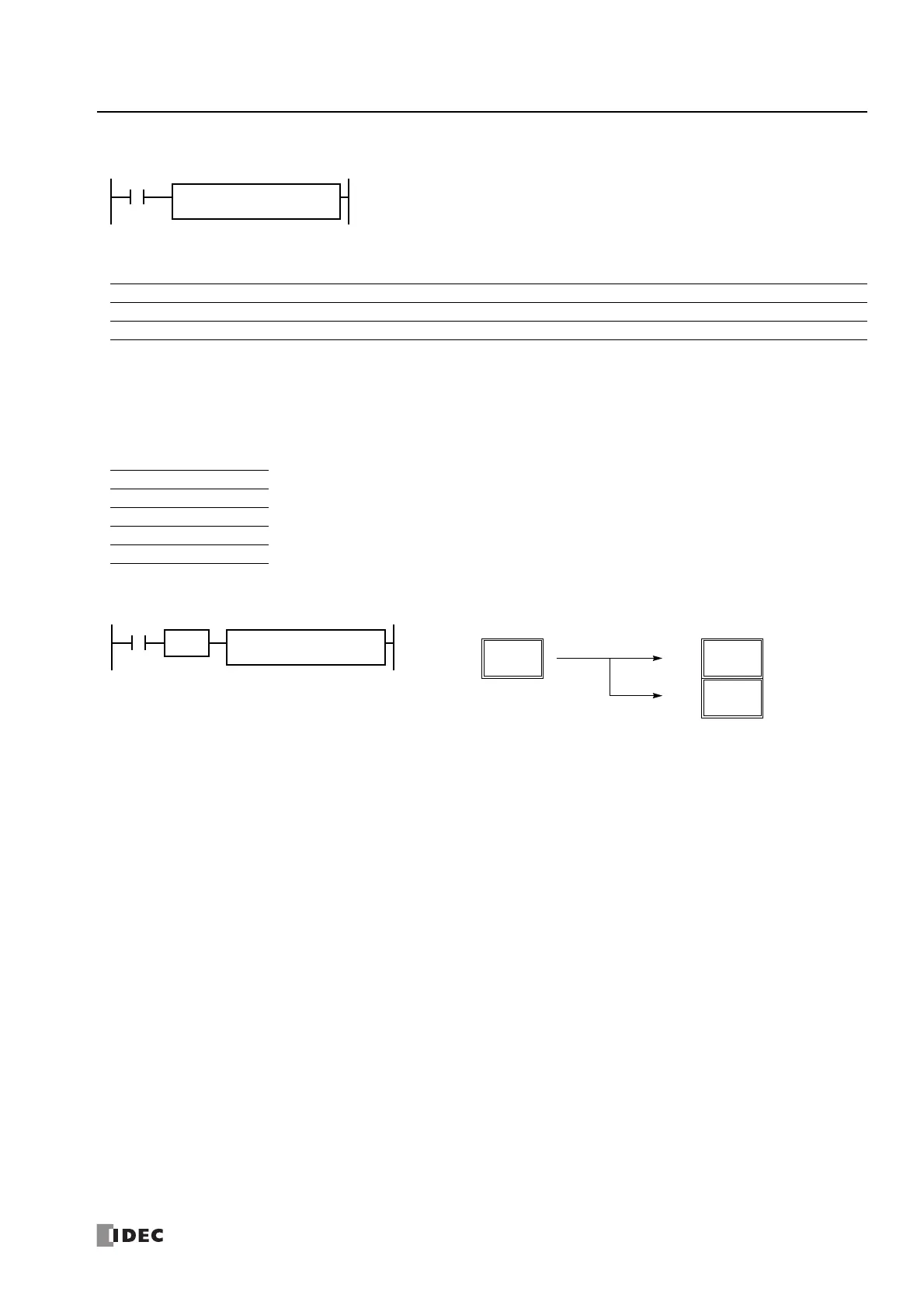
Example: DTDV
S1 → D1, D1+1
When input is on, the 16-bit binary data assigned by S1 is divided into upper and lower bytes. The
upper byte data is stored to the destination assigned by device D1. The lower byte data is stored to
the device next to D1.
Device Function I Q M R T C D P Constant Repeat
S1 (Source 1) Binary data to divide X X X X X X X — X —
D1 (Destination 1) Destination to store results — — — — — — X — — —
W (word) X When a bit device such as I (input), Q (output), M (internal relay), or R (shift register) is assigned as the source,
16 points (word data) are used.
When a word device such as T (timer), C (counter), or D (data register) is assigned as the source or destination,
1 point (word data) is used.
I (integer) —
D (double word) —
L (long) —
F (float) —
D1
D20
S1
D10
I1
DTDV(W)
SOTU
48
D20
(30h)
Before Execution
12345
D10
(3039h)
After Execution
57
D21
(39h)
Upper byte
Lower byte
 Loading...