8A3xxxx 144BGA EVK User Manual
© 2019 Integrated Device Technology, Inc.
List of Figures
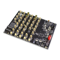
Figure 1. Overview of 144BGA ClockMatrix Evaluation Board ...........................................................................................................................4
Figure 2. Example of Voltage Jumpers ...............................................................................................................................................................5
Figure 3. GPIO Setting and Status Display Area ................................................................................................................................................7
Figure 4. Board Setting for Default Operation ....................................................................................................................................................8
Figure 5. Starting Up Timing Commander GUI ...................................................................................................................................................9
Figure 6. Selecting 8A34001 using Personality File v4.6 ..................................................................................................................................10
Figure 7. Timing Commander GUI with a Settings File Opened .......................................................................................................................11
Figure 8. Setting I
2
C for Connecting the Board with GUI ..................................................................................................................................12
Figure 9. A Green Band appears when a Valid Connection is Made ................................................................................................................12
Figure 10. Firmware Version Mismatch Warning Message ................................................................................................................................13
Figure 11. Reading Firmware Version ................................................................................................................................................................13
Figure 12. Read Firmware Version of ClockMatrix Chip .....................................................................................................................................14
Figure 13. AC Coupling and Terminations for Input Clock ..................................................................................................................................15
Figure 14. Configuring CLK0 as CMOS to Receive a 1PPS Input ......................................................................................................................15
List of Tables
Table 1. GPIO Settings ......................................................................................................................................................................................6
Table 2. EEPROM I
2
C Connections ..................................................................................................................................................................7
 Loading...